What is the Graphene Flagship?
Bringing together 118 academic and industrial partners in 12 research and innovation projects and 1 coordination and support project, the Graphene Flagship initiative will continue to advance Europe’s strategic autonomy in technologies that rely on graphene and other 2D materials. The initiative, which builds on the previous 10-years of the Graphene Flagship, is funded by the European Commission’s Horizon Europe research and innovation programme. The 2D-Experimental Pilot Line, addressing the challenges of upscaling 2D material production processes for the semiconductor industry, is another key component of the Graphene Flagship eco-system.
What's new

Sustainability in Graphene
Graphene and related 2D materials can advance the all 17 of the United Nations Sustainable Development Goals.

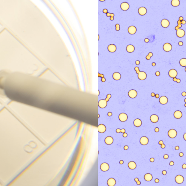
2D-EPL OFFERS A NEW EXPERIMENTAL MPW FROM GRAPHENEA SEMICONDUCTOR
Multi project wafer (MPW) runs are a common practice within the semiconductor ecosystem. Universities, R&D centres and start ups, which usually only need a few prototypes and operate with tight budgets, take advantage of this service to obtain devices at an affordable entry point. This is carried out with a mask sharing scheme, where devices with different geometries but shared device architecture are manufactured within the same mask; in this way, everyone gets a few devices but no one needs to purchase more devices than necessary. Now, Graphenea partners with the 2D Experimental Pilot Line (2D-EPL) to offer an MPW run with a novel process flow.

Call for Abstracts OPEN!
Your science, our future.
Join us at Graphene Week 2024, an international platform where research and innovation meet collaboration. Submit your abstract on graphene and 2D materials for a chance to present, discuss and connect with like-minded professionals.

Apply for our latest MPW run
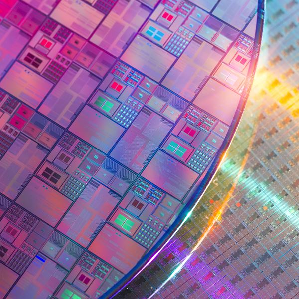
In the framework of 2D-EPL project several experimental multi-project wafer (MPW) runs are provided where universities, research institutes and companies can include their designs as dies on joint wafers.The offered process for the sixth MPW run is a photonic module combined with a graphene module.
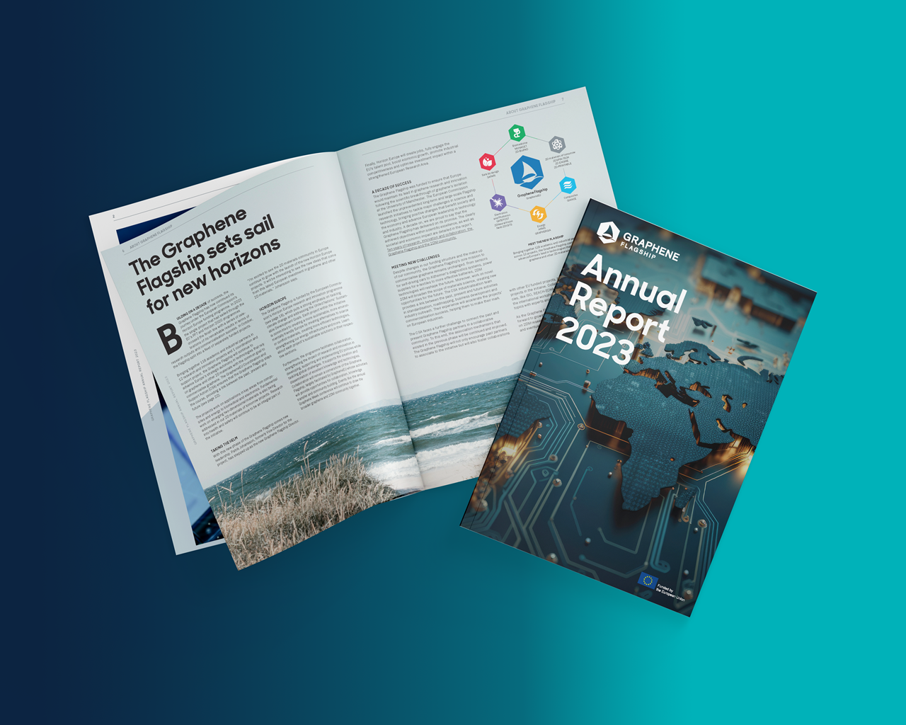
Annual Report 2023
The Graphene Flagship has continued its voyage in Horizon Europe. The latest Annual Report introduces our 13 new projects, provides updates on the 2D-Experimental Pilot Line's latest work and delves into the current state of 2D materials research and innovation in Europe.
Read our interactive report here or download the report here to learn about all about the next phase of the Graphene Flagship's journey.
Events

Graphene Week 2024
Standardisation Workshop
Advanced materials, such as nanomaterials, 2D materials, or thin films, play a crucial role in driving economic development and addressing major challenges in the coming years. These challenges include mitigating the impact of climate change, advancing lightweight engineering, enhancing catalysis, and improving medical applications. To comprehend the performance of these materials and ensure their acceptance across various sectors as safe and sustainable for both humans and the environment, the availability of reference procedures, materials, and data is essential. One versatile tool for establishing such references and evaluating the proficiency of individual laboratories and their competencies is through (international) interlaboratory comparisons (ILC). Notably, initiatives like the Versailles Project on Advanced Materials and Standards (VAMAS) provide a platform for conducting ILCs. This webinar will showcase various examples of interlaboratory comparisons, illustrating their impact on the development of reference products.
Pioneering 2D Materials for Semiconductor Industry
This free, lunch-to-lunch event will celebrate the 2D Experimental Pilot Line (2D-EPL) results and its progress towards creating an ecosystem for 2D materials integration in semiconductors for electronics, photonics, sensors and biomedical devices. The symposium will focus on photonics and biomedical applications and the benefits and challenges of industrial uptake for these technologies.