2D-EPL: Wafer scale growth
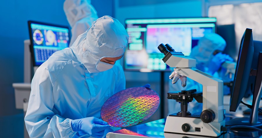
The Wafer Scale Growth Work Package aims to scale up the growth of high-quality single crystalline graphene and related 2D materials to 300 mm substrates and to provide the 2D films for the 2D Experimental Pilot Line (2D-EPL) processes.
This year’s progress
In this first year of the project, a new deposition system for the growth of 2D materials has already been designed and will be built and delivered to project partner imec in 2022. This prototype system is an essential part of the 2D-EPL, as it will allow the production of the highest quality 2D-material-based 300 mm wafers for the production of optoelectronic devices in the semi-industrial form factor. This system will be capable of controlled and uniform growth of 2D materials like graphene, hBN and transition metal dichalcogenides (TMDCs) like WS2 on sapphire and metal catalyst substrates in a fully automated way.
The biggest accomplishment this year is staying on track with all work package objectives despite the challenges of the Covid pandemic working conditions and long lead-times on components. The work package has 77 people working on process developments and plant development; the reduced interactions in remote work conditions and a lack of access to labs slows progress on assembly and testing.
Unexpectedly, our work on the design phase of the prototype development led to a technology change from a planetary reactor type to a close-coupled showerhead reactor type. This change should allow for an improved control of the growth of GRMs.
This work package will scale up the growth of high-quality single crystalline graphene for use in 2D-EPL processes.
Collaboration
Within the ecosystem of the Graphene Flagship, there is an intensive knowledge exchange and discussions on 2D material growth and characterization which is fruitful for further technology developments and process investigations.
What’s in store
The new 300 mm prototype deposition system for 2D materials, being developed by our work package, will be TRL level 7. It will be an essential part of achieving the 2D-EPL’s goal of establishing an ecosystem that is integrated in a commercial semiconductor foundry (TRL 7-8). After the project, work will continue on the prototype system to develop a commercial product for CMOS market application.
The new 300 mm prototype deposition system for 2D materials, being developed by our work package, will be TRL level 7. It will be an essential part of achieving the 2D-EPL’s goal of establishing an ecosystem that is integrated in a commercial semiconductor foundry (TRL 7-8).
AIXTRON, Germany