

What is the Graphene Flagship?
Bringing together 126 academic and industrial partners in 13 research and innovation projects and 1 coordination and support project, the Graphene Flagship initiative will continue to advance Europe’s strategic autonomy in technologies that rely on graphene and other 2D materials. The initiative, which builds on the previous 10-years of the Graphene Flagship, is funded by the European Commission’s Horizon Europe research and innovation programme.

What's new

Graphene-based innovation enters the leather industry through BeDimensional-Dermacolor collaboration
Graphene Flagship partner BeDimensional has partnered with Dermacolor to bring two-dimensional materials into leather manufacturing, demonstrating how advanced materials can improve performance in one of Europe's most established industrial sectors.

New Graphene Flagship project e-FLOWER aims to transform sustainable wearable electronics
Four-year Horizon Europe project will develop flexible, durable and circular e-textiles combining advanced materials, scalable manufacturing and user-centred design

2D Pilot Line offers PDKs
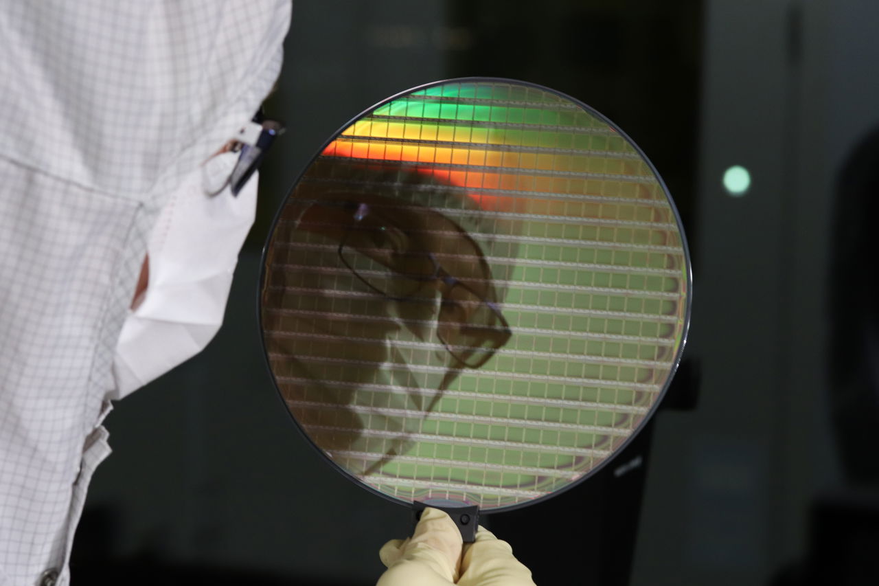
2D-PL Process Design Kits (PDKs) give you the building blocks, design rules and device models you need to turn innovative 2D material concepts into solid IC designs, to simulate physical data and realistic performances of next-generation devices.

Events

Seminar: Integration workflows for 2D material-based devices

Hands-on PDK training on IC design and simulation of 2D materials-based photonic devices
Join us from 2–4 November 2026 for a three-day hands-on training on design practices for 2D material-based photonic integrated circuits (PICs) on KLayout. This course will guide participants from fundamental concepts and design tools to more advanced implementations and exercises for photonic device architectures using our 2D-PL partners’ four diverse PDKs. The event will be held at imec in Leuven, Belgium, and carried out by expert designers involved in the EU-funded project 2D-PL, a part of the Graphene Flagship initiative, and co-hosted by EUROPRACTICE.

2D-PL @ SEMICON Europa 2026
At SEMICON Europa, the 2D Pilot Line (2D-PL) project showcased its work driving the next phase of Europe’s semiconductor innovation by advancing the integration of 2D materials into photonics and electronics. This initiative focuses on providing end-to-end prototyping services for the integration of graphene and transition metal dichalcogenides (TMDCs) into established silicon-based platforms. The 2D-PL aims to bring 2D material (2DM) fabrication closer to industrial readiness by developing and validating processes in a FAB-relevant environment. Its module development is focused on photonic and electronic devices and circuits, addressing the needs of research organisations, SMEs, large companies, integrated device manufacturers (IDMs) and foundries across Europe.
