Jump to content

2D-PL multi-project wafer run 2


EU Funded

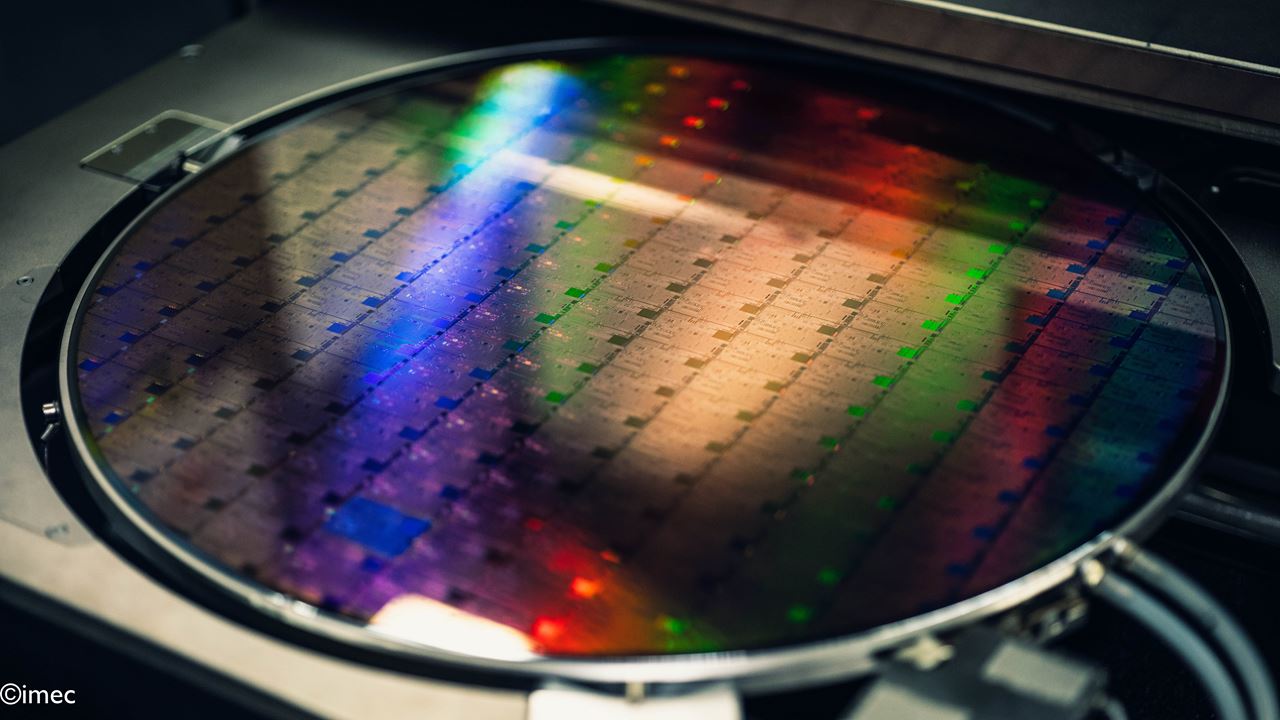
IHP – Leibniz Institute for High Performance Microelectronics, focuses on the development of graphene photonic integrated circuits (PIC) in a 200 mm pilot line. This involves exploring various integration aspects for the realisation of integrated devices. The process flow is based on graphene photonic module on 200 mm Si wafers and enables a fabrication of proof-of-concept devices like graphene electro-absorption modulators, Mach-Zehnder interferometers or micro ring resonators. Design rules will include the basic design elements to be used in this particular e-MPW run.

More details on the PDK can be found here.

KEY BENEFITS
  • Graphene-based PICs combined with embedded SiN waveguides
  • Testing of diverse components for advanced high-speed communication, optical computing, etc. systems.
  • Device designs can be adapted within defined process specifications for photonic and graphene modules.
KEY FEATURES
  • Fabrication of Graphene photonic devices in 200 mm BiCMOS pilot line with tailored processes
  • Preliminary device libraries including waveguide, grating coupler, modulator performances

Process flow

The e-MPW process flow is built on Dual Layer graphene electro-absorption modulator flow. The process includes essential modules such as contact, waveguide, and coupler modules, along with specialized graphene integration for enhanced functionality. Cladding and encapsulation modules ensure optical confinement and device protection. Finally, metal heaters could be implemented in the flow.


Process Step

Process/Layer

Material

Thickness

0

Bottom Cladding (BOX)

SiO2

1200 – 2600 nm

1

Met1 Layer

Ti/TiN/AlCu/Ti/TIN

480 – 530 nm

2

Oxide layer and CMP

SiO2


3

Waveguide

SiN

400 nm

4

Via opening


5

Grating coupler

SiN


6

Graphene Layer

CVD Monolayer Graphene


7

Spacer Layer

SiN

20 – 40 nm

8

Graphene Layer

CVD Monolayer Graphene


9

Passivation Layer

SiN

20 nm

10

Top Cladding

SiO2

500 – 2100 nm

11

Pad opening


12

Top Heaters

Various Metals

20-60 nm


PRICE

  • 8000 € fixed entry price
  • 300 €/mm2 for the industry customers and 200 €/mm2 for academic customers
  • 10 dies will be delivered by default
  • 50% discount is available through the 2D-PL support programme

IMPORTANT DATES
If you are interested in any of our capabilities, please contact us at 2DPL@graphene-flagship.eu. Whether you are exploring a new concept or have a specific process in mind, our team can help assess your project's feasibility, discuss technical requirements, and identify the most appropriate fabrication route.

ACCESS

Both the PDK and the fabrication services are enabled following the signature of the IHP Non-Disclosure Agreement (NDA). The PDK is available free of charge to interested parties. For more information or to request access to the services, please contact 2DPL@graphene-flagship.eu.

 This run is now closed.

wafer production

Reduced fees

The 2D-PL Support Programme lowers the obstacles for researchers and companies wanting to join our multi-project wafer (MPW) runs. Selected participants can receive a reduction of up to 50% off the MPW fee in exchange for providing feedback on the received devices in the form of a short interview with the hosting pilot line. Your feedback helps us improve future runs. 

2D-PL support programme
IHP

About IHP

IHP focuses on research and development in the field of microelectronics and information technology, in particular on the promotion of silicon-based high technologies to strengthen microelectronic research and industry in Germany and Europe. The spectrum of research work ranges from innovative materials to complex systems, e.g. for communication, which is a unique selling point in the research landscape. IHP covers the entire R&D value chain, from basic research to the manufacturing of prototypes and small series. The basis for IHP's capabilities is the institute's own continuously (24/7) operated pilot line with its qualified 0.25/0.13 µm SiGe BiCMOS technologies.

Currently, graphene, with its potential for functional extension of Si technology, is one of the research fields at IHP. The research includes material synthesis on 200 mm wafers in the IHP’s cleanroom and development of technological processes for graphene device fabrication in a 200 mm pilot line.