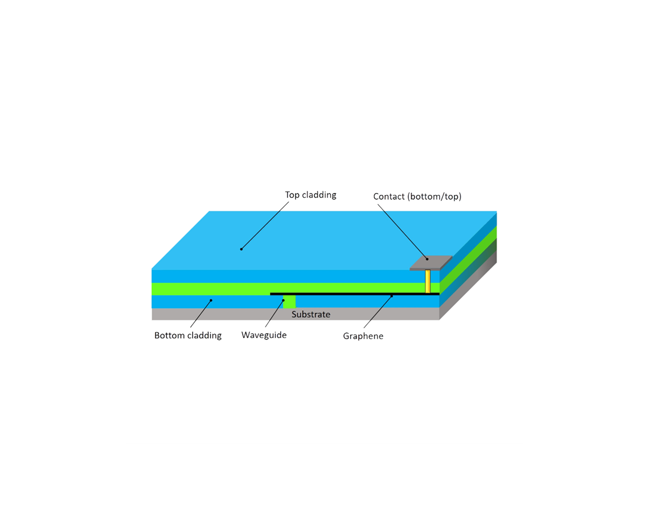
Specifications
Substrate
- Material: Silicon
- Waveguide: Silicon Nitride
Resolution
- 1 um
Modules:
- Contact module
- Waveguide module
- Coupler modules
- Graphene Module
- Encapsulation module
- Cladding modules
Application:
- Photonics


In the framework of 2D-EPL project several experimental multi-project wafer (MPW) runs are provided where universities, research institutes and companies can include their designs as dies on joint wafers. This run is mainly intended for graphene photonics and will be offered by IHP – Leibniz Institute for High Performance Microelectronics.
The offered process for the fifth MPW run is a photonic module combined with a graphene module. The design of the device can be adjusted within the specifications listed below.
Important Dates:
Price:

Substrate
Resolution
Modules:
Application:

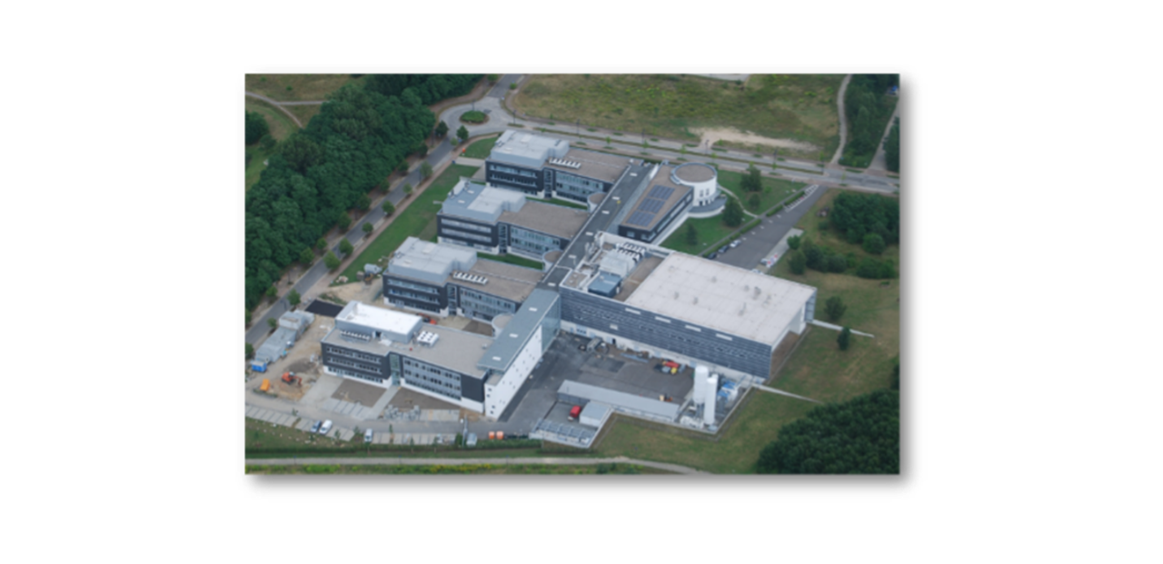
IHP focuses on research and development in the field of microelectronics and information technology, in particular on the promotion of silicon-based high technologies to strengthen microelectronic research and industry in Germany and Europe. The spectrum of research work ranges from innovative materials to complex systems, e.g. for communication, which is a unique selling point in the research landscape. IHP covers the entire R&D value chain, from basic research to the manufacturing of prototypes and small series. The basis for IHP's capabilities is the institute's own continuously (24/7) operated pilot line with its qualified 0.25/0.13 µm SiGe BiCMOS technologies.
Currently, graphene, with its potential for functional extension of Si technology, is one of the research fields at IHP. The research includes material synthesis on 200 mm wafers in the IHP’s cleanroom and development of technological processes for graphene device fabrication in a 200 mm pilot line.