Full process details
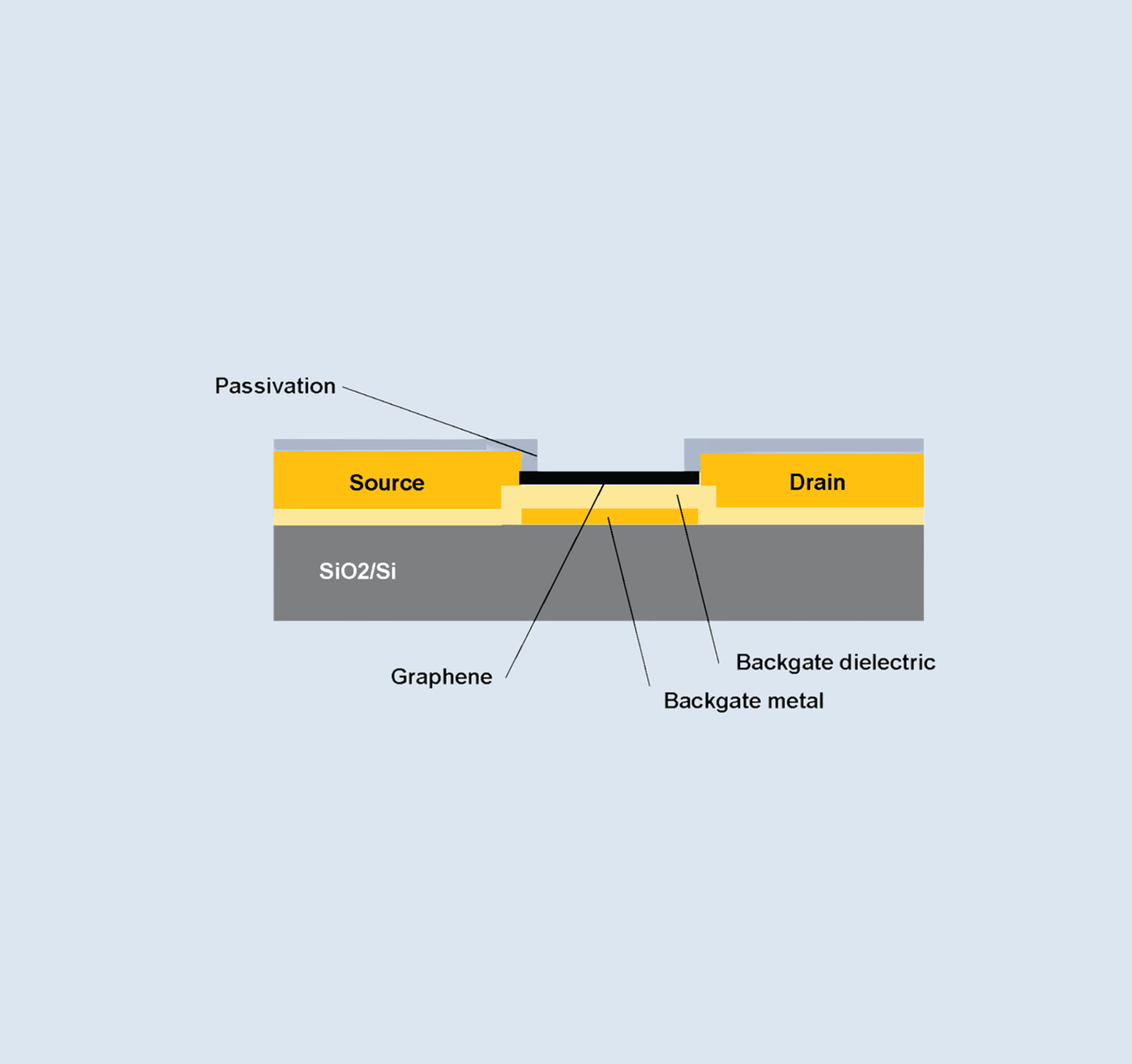
Backgate metal: Ti/Au 5/15
Backgate dielectric: HfOx 20nm
Graphene: CVD grown >97% monolayer
Metal S/D contact: Au 50nm
Passivation dielectric: AlOx 50nm
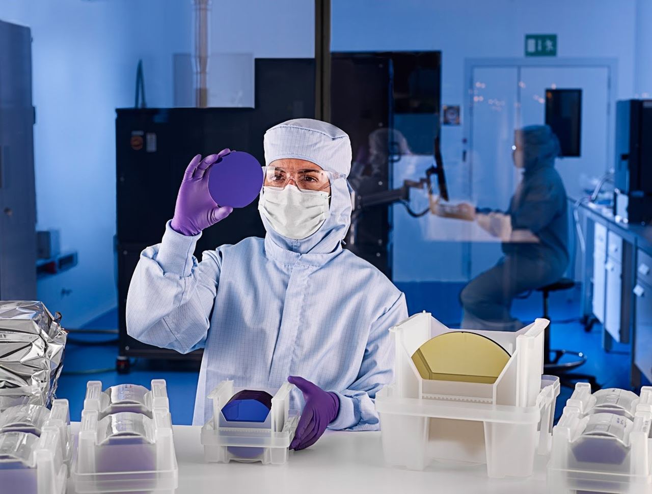
The 2D-EPL project is launching its sixth multi-project wafer (MPW) run where universities, research institutes and companies can include their designs as dies on joint wafers. This run, provided by Graphenea Semiconductors, provides a flexible platform into which we can implement three different types of devices within one process flow. Applications can range from general electronics and sensing to optoelectronics.
3900€ for 4 cm2 (4x 1x1cm2 dies or 16x 5x5mm2 dies)
Backgate metal: Ti/Au 5/15
Backgate dielectric: HfOx 20nm
Graphene: CVD grown >97% monolayer
Metal S/D contact: Au 50nm
Passivation dielectric: AlOx 50nm
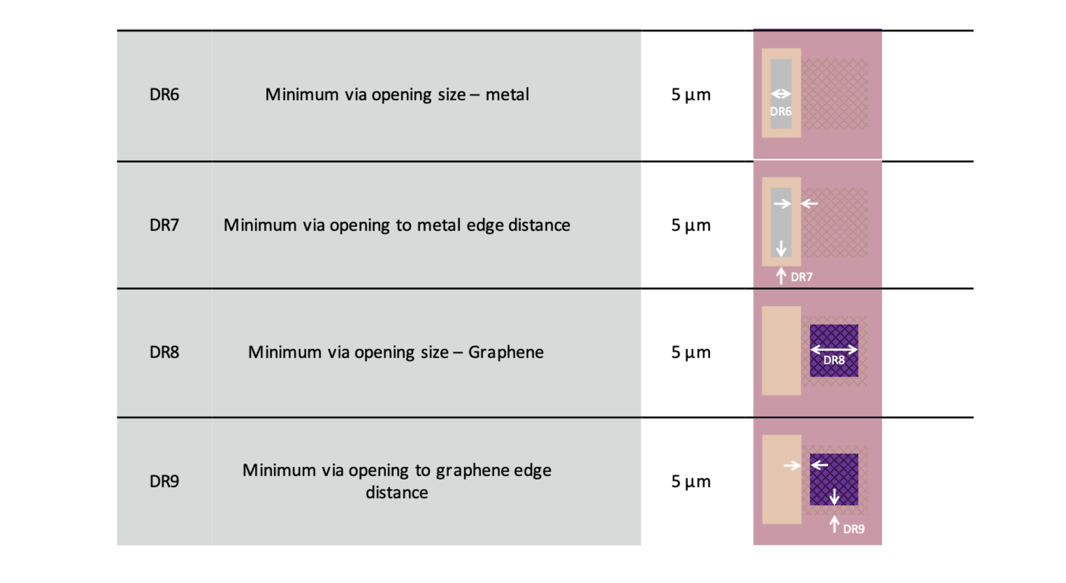
Comprehensive set of Design Rules for device design on .gds format files
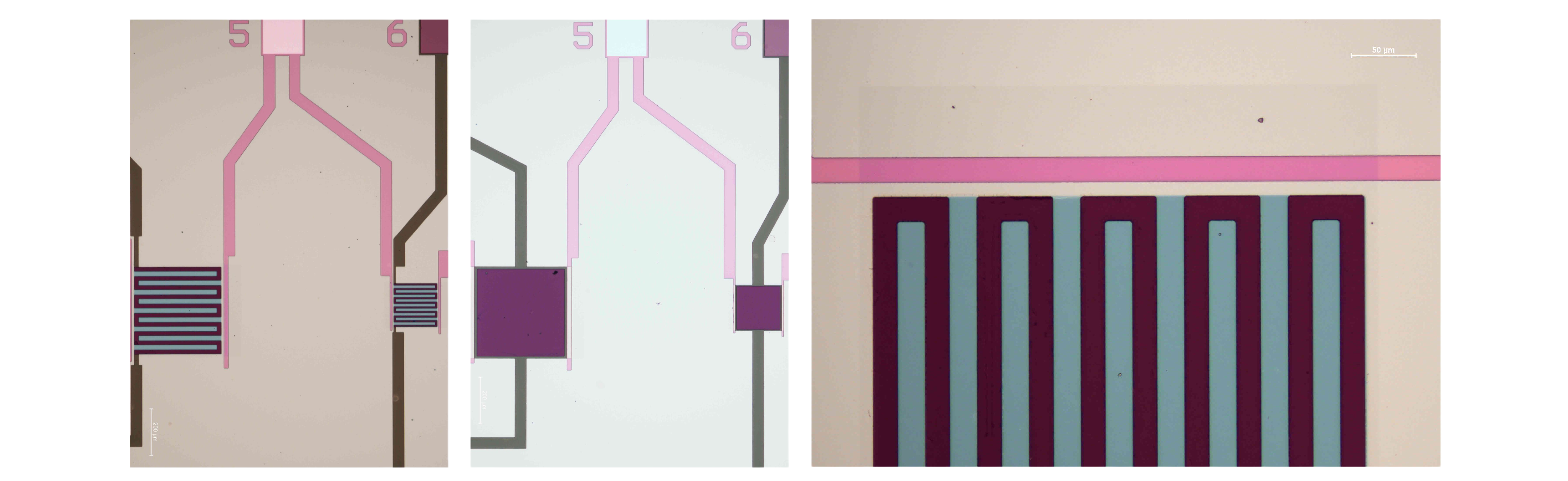
Images left to right: a) 4 terminal devices with local heaters and passivated electrodes (5x magnification); b) 3 terminal devices with local gates and passivated electrodes (5x magnification); c) 3 terminal devices with local heaters and passivated electrodes (20x magnification).
Graphenea, a technology company founded in 2010, is a world leading graphene producer. The 25 employees in Graphenea work on contributing to the successful development of graphene applications of our customers, in a wide range of sectors and in more than 60 countries in the world. Through research and innovation, we support our customers with our portfolio consisting of: CVD Graphene films, Graphene Field-Effect-Transistors chips (GFETs), Graphene Foundry Services (GFAB) and Graphene Oxides. Graphenea’s facilities are located in Spain (San Sebastián) and USA (Boston).