Electronics & Photonics
Due to the interesting electronic and optical properties of graphene and 2D materials, it is obvious that many different applications are possible in this field. This field often requires thin films and layered materials, which represents a paradigm change compared to bulk utilizations of 2D materials. The market perspective is generally very promising, as large and typically growing markets are addressed.
A major obstacle for many applications is economic feasibility of wafer scale integration and scalable high quality preparation of graphene and other 2D material films with sufficient quality and yield. On the other hand, if wafer scale integration succeeds, many applications suddenly become interesting and viable.
In terms of applications from a functional point of view, hybrid approaches with silicon appear promising, where graphene is added in the back-end-of-line or back end to deliver additional functionalities (e.g. optoelectronics, THz, sensors). Besides that, 2D materials appear particularly interesting for flexible applications where no leading incumbent technology readily exists (silicon does not perform well) and, thus, a strong need for new materials persists.
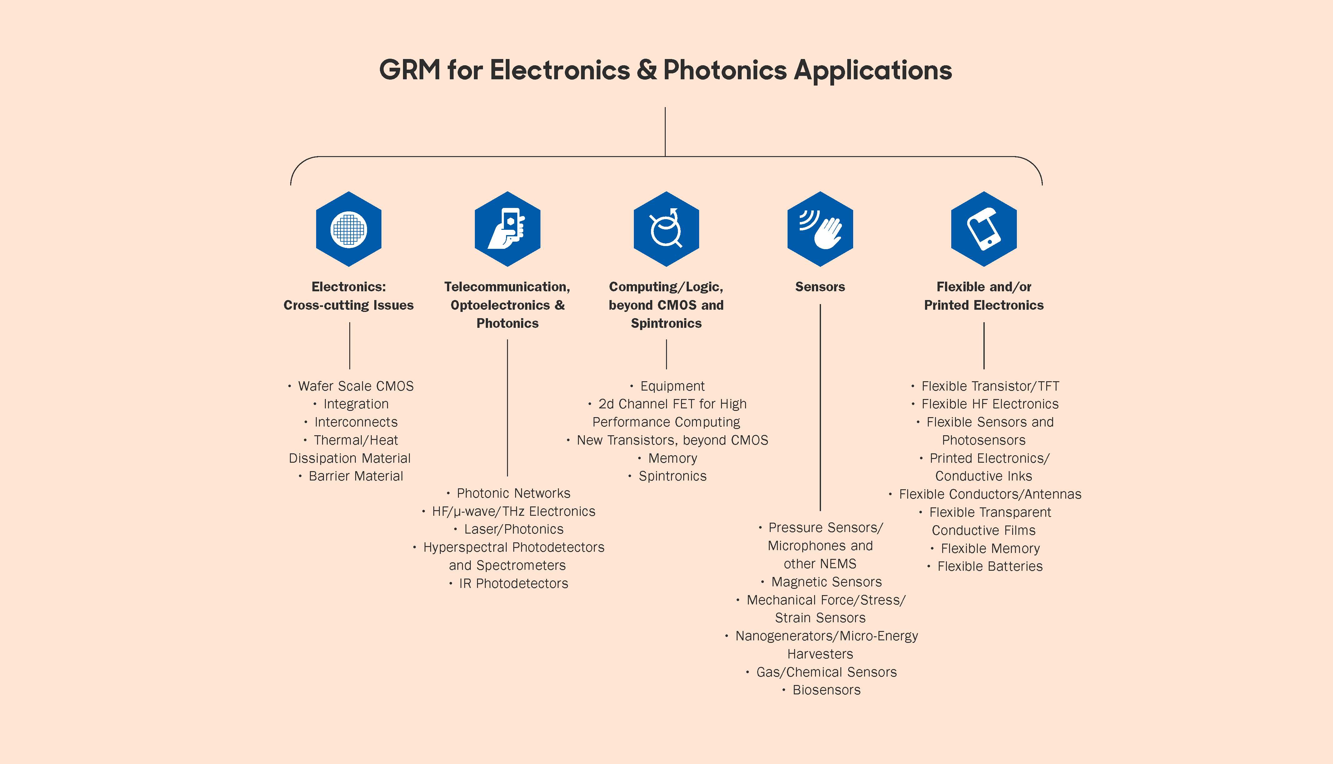
This table illustrates the various uses for graphene and related materials (GRM) for electronics and photonics applications.