Jump to content

2D-EPL multi-project wafer run 3


EU Funded

The 2D-EPL's third MPW run is mainly intended towards electronics but can also include sensor devices (e.g. Hall sensor, but via opening on graphene is not in the scope of this run) and will be provided by AMO GmbH. The design of the device can be adjusted within the specifications. The offered device structure is a GFET (Fig. 1) consisting of the following fabrication steps:

  • Back gate
  • Dielectric deposition & vias opening
  • Fabrication of adhesion pads
  • Wafer scale graphene transfer & patterning
  • Top contacts fabrication
  • Encapsulation & vias opening (not on top of graphene)

Timeline

Application Phase: 1 April– 18 June 2023

Final Layout Submission and PO: 25 June 2023

MPW Run 3: 1 October – 30 November 2023

Delivery: 1 December 2023 – 21 January 2024

  • During the application phase, interested clients can contact us via the contact form and receive further information about the run in a first meeting.
  • Final Layout Submission and PO must be received by 25 June.
  • The chips are expected to be delivered in December 2023.

Pricing

  • 1300€ set price for four dies with identical design (1x1 cm²)
  • 250€ for each additional die with identical design 


  This MPW run is now closed. Stay tuned for our next run, opening soon.

View full specifications

Figure 1. Scheme with the different layers of the final GFET structure.

The summary of the key parameters for a device with local back gate is shown in the table below:

Table with MPW run 3 specifications

Specifications

Substrate

  • Material: Silicon
  • Basic die size: 1 x 1 cm²

Resolution

  • General design rule: 10 μm for in-layer critical dimension and over-layer alignment

Table with description of the MPW run 3 GFET layers and thicknesses

Characterisation

  • Raman characterisation
  • Electrical measurement for as-fabricated reference devices
  • General optical inspection of your devices

This MPW run is now closed. Stay tuned for our next run, opening soon.

Map of Europe with Aachen called out with an image of the AMO building

About AMO

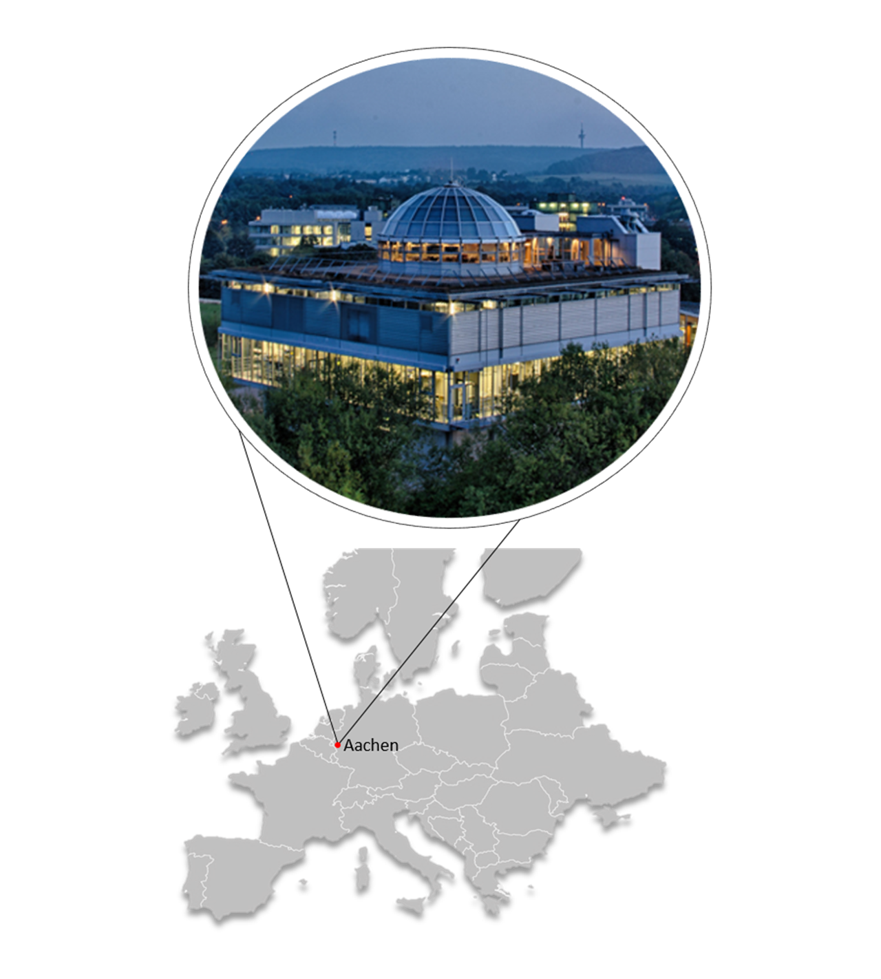
Located in Aachen, Germany, close to the borders of Belgium and the Netherlands, the research foundry AMO GmbH, a non-profit nanotechnology SME, follows the mission to efficiently close the gap between university research and industrial application. It demonstrates innovative technologies and introduces new materials, including their implementation in novel device architectures, prototyping and small volume fabrication. A state-of-the-art 400 m² cleanroom is operated and a range of services from consulting to prototype development is offered. In recent years, AMO has become a global player in 2D materials research for electronics and photonics.