


Making structures on 2D materials with a 3D printer
A new method for creating nanopatterns on layered materials
In the quest to leverage the exceptional properties of graphene and other 2D materials, researchers at Graphene Flagship Associated Member KTH Royal Institute of Technology (Sweden) and Graphene Flagship Partner the University of the Bundeswehr Munich (Germany) & SENS Research Center joined forces to structure 2D materials using direct writing with the built-in laser of a commercial two-photon 3D printer. Published in ACS Nano, the technique worked on platinum diselenide, molybdenum disulfide, and graphene grown on or transferred to borosilicate glass coverslips.
Traditional methods, such as optical lithography and laser interference lithography, require coating the 2D material with a protective resist mask, allowing only specific areas of the 2D material to be exposed during etching. However, the process of coating, developing, and removing the photoresist can damage the 2D material.
The technique presented in the study does not require a masking layer, thereby avoiding contamination and damaging the substrate. To structure the 2D materials, the researchers used an oil immersion objective and a transparent substrate. The team was able to generate nanoholes (≥100 nm diameter) in a 200 μm × 200 μm area in just a few seconds.
The work is particularly interesting because it allows scientific and industrial players without access to standard microfabrication facilities to explore new concepts and devices based on 2D materials. Since two-photon 3D printers are becoming cheaper and more common in research labs and companies, this method can be used to fast-prototype and manufacture new 2D material-based devices in various research fields.
“Providing a way to work with 2D materials outside the cleanrooms lowers the bar for engaging in this exciting field of research,” says Alessandro Enrico, one of the study’s lead authors, who used to work at the Division of Micro and Nanosystems (MST) at KTH and recently transferred to the University of Pavia in Italy. “This approach has other advantages over conventional lithographic processes: the material is not damaged or contaminated by multiple steps of coating and solvent rinsing. No chemical also means a more environment-friendly approach for 2D material research and production,” adds the researcher.
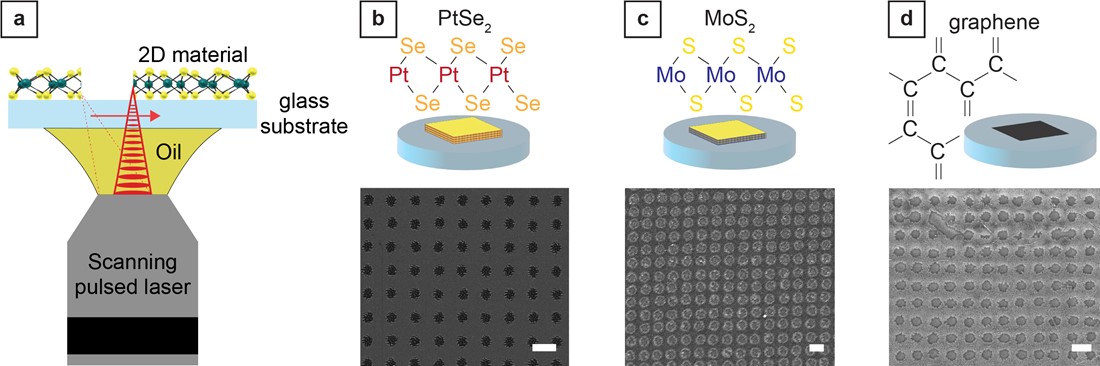
Nanopatterning of 2D materials using a two-photon 3D printer. (a) 3D schematic of the laser writing approach. The 2D material is either grown or transferred on the front side of a thin glass coverslip. (b), (c), and (d) present nanohole arrays in platinum diselenide (PtSe2), molybdenum disulfide (MoS2), and graphene, respectively. Scale bar, 1 μm for PtSe2, 500 nm for MoS2, and 300 nm for graphene.
The next step is to investigate the compatibility of this method with suspended 2D material membranes and replace the glass substrate with other functional ones.
This project was done within the Graphene Flagship and the Graphene Flagship Partnering Project FLAG‐ERA JTC 2019 2D‐NEMS, which is affiliated with the Sensors Work Package of the Graphene Flagship.
Reference
Enrico, Alessandro, et al. "Ultrafast and Resist-Free Nanopatterning of 2D Materials by Femtosecond Laser Irradiation." ACS nano 17.9 (2023): 8041-8052. https://pubs.acs.org/doi/full/10.1021/acsnano.2c09501
Author bio

Letizia Diamante
Science Writer and Coordinator of the 'Diversity in Graphene' initiative.