Scalable 100% yield production of conductive graphene inks
Conductive inks based on graphene and layered materials are key for low-cost manufacturing of flexible electronics, novel energy solutions, composites and coatings. A new method for liquid-phase exfoliation of graphite paves the way for scalable production.
Conductive inks are useful for a range of applications, including printed and flexible electronics such as radio frequency identification (RFID) antennas, transistors or photovoltaic cells. The advent of the internet of things is predicted to lead to new connectivity within everyday objects, including in food packaging. Thus, there is a clear need for cheap and efficient production of electronic devices, using stable, conductive and non-toxic components. These inks can also be used to create novel composites, coatings and energy storage devices.
A new method for producing high quality conductive graphene inks with high concentrations has been developed by researchers in the Graphene Flagship, led by researchers at the Cambridge Graphene Centre at the University of Cambridge, UK, in collaboration with researchers at the Bruno Kessler Foundation, Italy and Queen Mary University of London, UK. The novel method uses ultrahigh shear forces in a microfluidisation process to exfoliate graphene flakes from graphite. The process converts 100% of the starting graphite material into usable flakes for conductive inks, avoiding the need for centrifugation and reducing the time taken to produce a usable ink. The research, published in ACS Nano, also describes optimisation of the inks for different printing applications, as well as giving detailed insights into the fluid dynamics of graphite exfoliation.
Printing layered materials
The inks produced by the microfluidisation process have high concentrations of up to 100 g of graphene flakes per litre. Using the most efficient rheology modifiers and stabilisers, the microfluidised graphene mixture is optimised for screen printing. Panagiotis Karagiannidis, a researcher at the University of Cambridge, is lead author of the work. "The motivation was the need for layers with low sheet resistance to be produced by screen printing using inks with high concentration," he said.
As well as graphene, this method can easily be applied to other layered materials, such as hexagonal boron nitride or transition metal dichalcogenides. This will provide a family of printable circuit components – conductor, insulators and semiconductors – with which to build a variety of printed electronics with different functionalities.
High yield inks
These high-yield inks contain a high concentration of chemically unmodified few-layer graphene, leading to excellent conductivity of the final printed material. The inks also give an excellent sheet resistance below 2 Ω/sq, suitable for RFID antennas and electrodes in optoelectronic or energy storage devices. These inks are ideal for applications where low-cost is important.
In the microfluidisation process, graphite powder is mixed with water and a surfactant is added to prevent flakes from aggregating. The mixture is passed through a microfluidiser, where it is forced at high pressure through a zig-zag shaped microchannel. Turbulent flow through the diamond-coated microchannel, leads to ultra-high shear rates of 108 s-1, exfoliating the graphite into few-layer flakes. Importantly, all of the input mixture flows through the microchannel and experiences the high shear, and the process can be repeated to achieve the required graphene flake sizes. "All of the starting mixture experiences the same uniform intensive shear levels, converting it into a usable ink with high concentration. There is no wastage of material or time consuming post-processing," added Karagiannidis.
Mar García-Hernandez of the Spanish National Research Council (CSIC) is the leader of the Graphene Flagship Work Package Enabling Materials, which is focused on development of scalable synthesis methods for graphene and other layered materials. "Microfluidisation is a huge leap ahead towards applications of affordable and environmentally friendly graphene inks in organic photovoltaics, RFID antennas, electrically conductive coatings or nanocomposites," she said. "The method is certainly well suited for the synthesis of a variety of other layered material inks, which will certainly enlarge the scope of applications of layered materials in real world devices."
Scalability
An important issue for the use of graphene inks in printed electronics and other applications is scalability – producing inks and dispersions in large enough quantities for industrial applications. With the 100% yield of the microfluidisation method, it is now possible to produce high quality graphene in sufficient quantities for commercial products.
Inks produced using this method have already been commercialised via a University of Cambridge spin out company, Cambridge Graphene, which was recently acquired by engineering solutions company Versarien. The inks are also supplied to Graphene Flagship partner Novalia, UK for use in their interactive touch-based printed electronic demos. Chris Jones of Novalia said "For viable marketable applications, the materials need to be cost effective, easy to handle and show consistent performance. We ran these inks on ordinary industrial screen printing equipment without modification and achieved consistent results, printing hundreds of interactive demonstrators for Mobile World Congress. This is a very exciting point - a critical juncture between the laboratory and the public."
Andrea Ferrari, Science and Technology Officer of the Graphene Flagship and Chair of its Management Panel, stated "This is an important conceptual advance, and will significantly help the innovation and industrialization goals of the Flagship. The fact that the process is already licensed and commercialized indicates how it is feasible to cut the time from lab to market even during the lifetime of the Flagship."
Further Reading
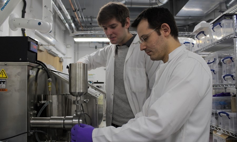
Banner image: Graphene ink part-way through the microfluidisation process, James Macleod/University of Cambridge Engineering Department, 2017.

This is a very exciting point - a critical juncture between the laboratory and the public."
Novalia


