Pioneering 2D Materials for semiconductor industry
Wafer Level Single Crystalline 2D Materials
One of the biggest challenges the 2D materials faces to be adopted by this industry is the growth of material with a similar stability, reliability and defect density. In this workshop we addressed and discussed these growth challenges.
Keynote speakers

Stephan Hofmann
Professor of Nanotechnology at the Dept. of Engineering at Cambridge University.

Hiroki Ago
Professor at the Global Innovation Center, Kyushu University, in Fukuoka, Japan.

Cedric Huyghebaert
Research Manager Nano Applications Material Engineering at imec

Sanna Arpiainen
Principal Scientist, Team Leader, VTT (Event Chair)

Amaia Zurutuza
Scientific Director at Graphenea (Moderator)
Stephan Hofmann
Stephan Hofmann is Professor of Nanotechnology at the Department of Engineering at Cambridge University, and Director of the NanoDTC Doctoral Training Centre in Nanotechnology. His research group works on the application driven exploration of new device materials, bridging from fundamental discovery and characterisation of properties to functional device integration and manufacturing pathways.
He graduated in Physics at the Technische Universität München and obtained his Ph.D. at the University of Cambridge. Prior to his faculty position, he held a Dorothy Hodgkin Fellowship by the Royal Society and a Research Fellowship at Peterhouse, Cambridge, where he is currently a Fellow.
Hiroki Ago
Prof. Hiroki Ago received his PhD from Kyoto University in 1997. After staying at Cavendish Laboratory, Cambridge University during 1997-1999, he moved to National Institute of Advanced Industrial Science and Technology (AIST), Tsukuba. In 2003, he moved to Institute for Materials Chemistry and Engineering, Kyushu University as an associate professor. He became a full professor of Global Innovation Center (GIC) of Kyushu University in 2016. He received Iijima Award from the Fullerene-Nanotube Research Society of Japan (2006), Young Scientist Award from the Minister of Education, Culture, Sports, Science and Technology (MEXT), Japan (2008), and Best Paper Award from the Japan Society of Applied Physics (2014).
About the workshop
One of the key success factors for the phenomenal rise of the semiconductor industry is the production of Si wafers with a defect density of roughly one defect over 10^14 Si atoms. This extremely low defect density provides the industry with a reliable, reproducible and stable material to build the most advanced devices. One of the biggest challenges the 2D materials faces to be adopted by this industry is the growth of material with a similar stability, reliability and defect density. In this workshop we addressed and discussed these growth challenges.
Agenda
11:00 - 11:15 | Cedric Huyghebaert
2D Experimental Pilot Line update
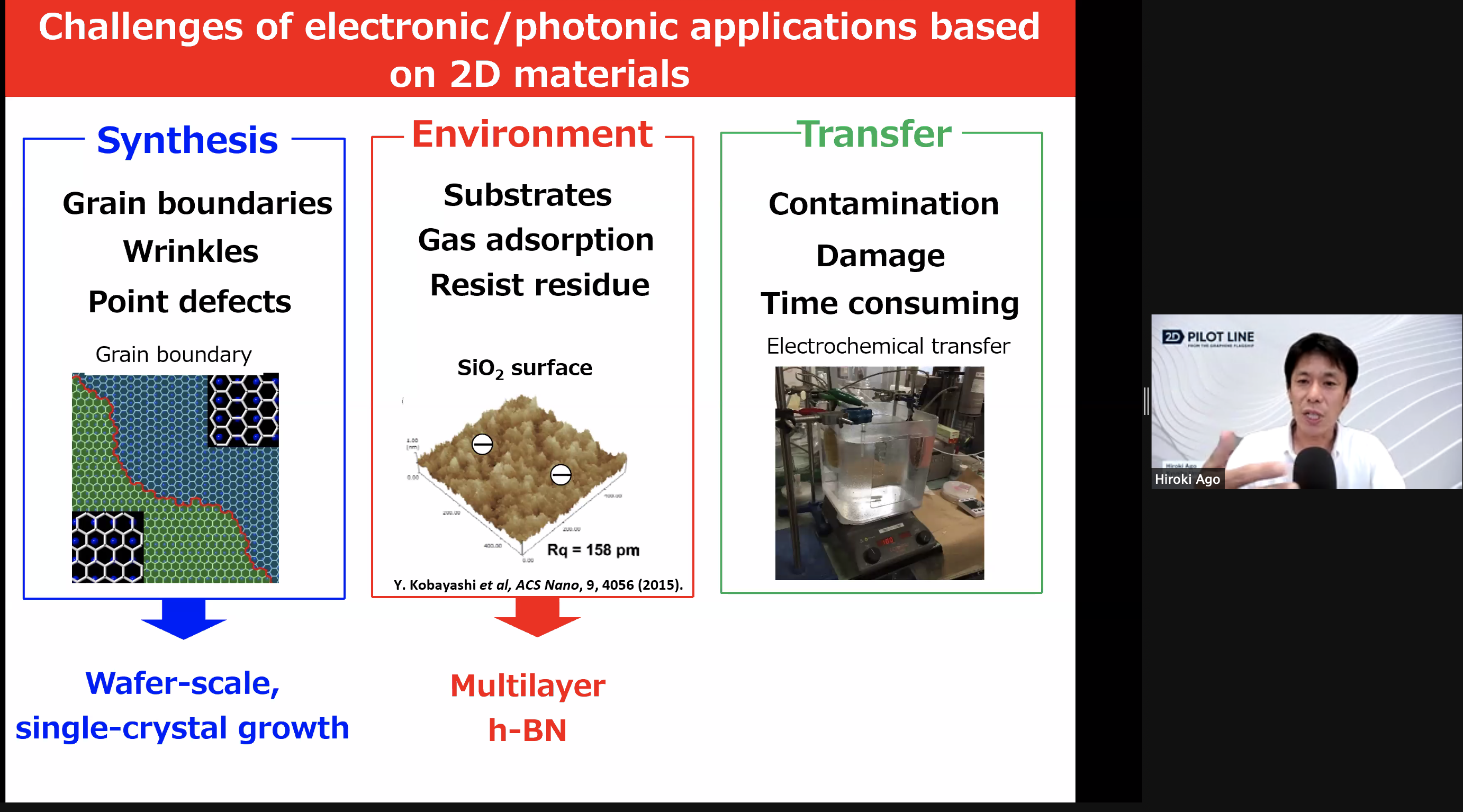
11:15 - 11:55 | Hiroki Ago
Controlled CVD Growth of High-Quality 2D Layered Materials for Electronic and Photonic Applications
The development of graphene research has opened the new field of atomically thin, 2D layered materials. For realizing various applications including high-performance electronic and photonic devices, it is very important to establish synthesis methods of high-quality, large-area 2D materials. We have been studying chemical vapor deposition (CVD) growth of monolayer and bilayer graphene and other related 2D materials, such as and hexagonal boron nitride (hBN) and transition metal dichalcogenides (TMDCs), with the main focus on the understanding of growth mechanisms as well as the growth of high-quality 2D films for advanced applications. In this talk, I will review our recent work on the highly controlled CVD growth and modifications of graphene, h-BN, and their heterostructures.
11:55 - 12:25 | Stephan Hofmann
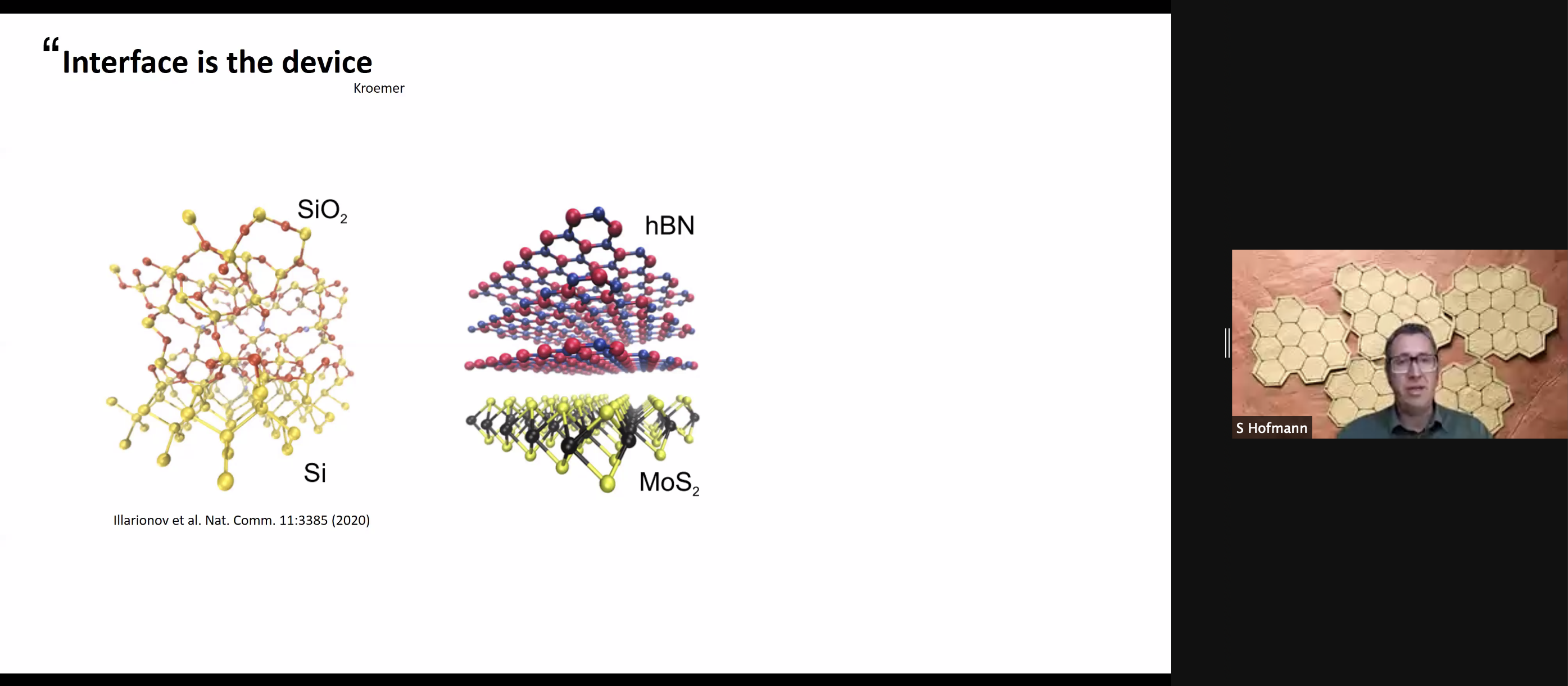
On the Fundamental Mechanisms that underpin Process Technology for Atomically Thin 2D Films
We systematically adapt in-operando metrology to understand the mechanisms that govern the growth, interfaces and device behaviour of 2D materials at the monolayer limit in realistic process environments, in order to accelerate their development cycles as scalable industrial materials particularly via chemical vapour deposition. The talk will focus on our recent results on graphene, hBN and WS2, highlighting the interdisciplinarity this comprises, ranging from metallurgy and new approaches to epitaxial metal growth to defect characterization by multi-dimensional super-resolution microscopy, machine-learning assisted materials discovery and new quality monitoring approaches at commercial scale.
12:25 - 12:55 | Panel Discussion
Growth challenges for the community and industry.
Moderator: Amaia Zurutuza
12:55 - 13:00 | Closure