Graphene Study 2023
Beyond graphene - additional 2D materials applications
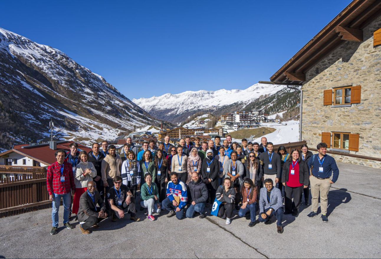
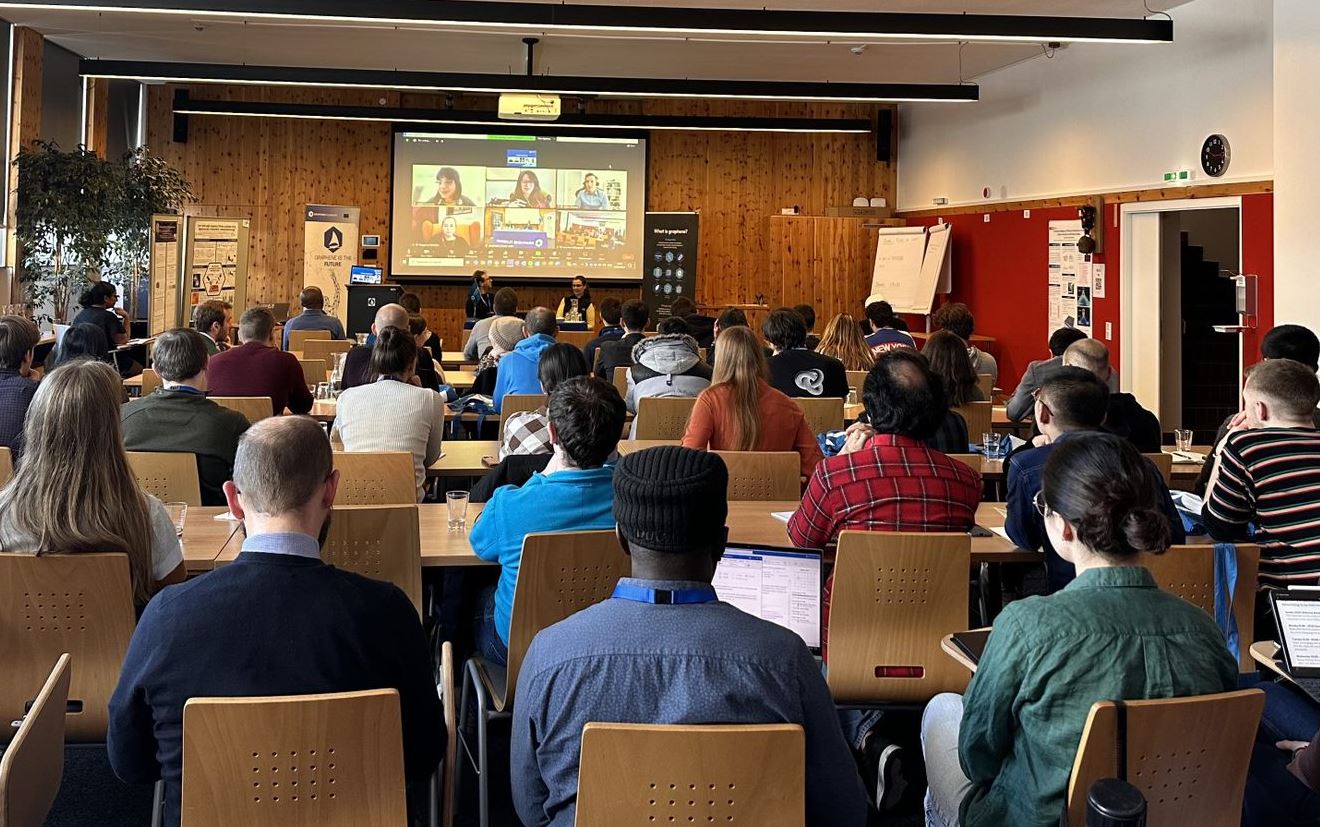
The Graphene Flagship hosts Graphene Study to help PhD students and early career researchers develop into outstanding researchers in graphene. This edition explored 2D materials for tomorrow. What is next? What can we expect from graphene science and applications in the future? View the full agenda below.
Graphene Study 2023 Speakers:

Kostya Novoselov

Patrik Johansson

Amalia Patane

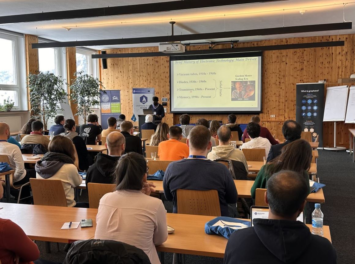
Deji Akinwande

Catherine Journet

Camilla Coletti

Luca Banszerus

Jamie Fitzgerald

Peter Bøggild

Alessandro Molle

Sofia Öiseth

Jean-François de Marneffe
Kostya Novoselov
Professor Sir Konstantin Novoselov FRS, foreign associate of the National Academy of Sciences, USA
Prof Sir Konstantin ‘Kostya’ Novoselov FRS was born in Russia in August 1974. He is best known for isolating graphene at The University of Manchester in 2004, and is an expert in condensed matter physics, mesoscopic physics and nanotechnology. Every year since 2014 Kostya Novoselov is included in the list of the most highly cited researchers in the world. He was awarded the Nobel Prize for Physics in 2010 for his achievements with graphene. Kostya is a director of the Institute of Functional Intelligent Materials and holds a position of a Tan Chin Tuan Centennial Professor at the National University of Singapore. He is also part time Langworthy Professor of Physics and the Royal Society Research Professor at The University of Manchester.
He graduated from the Moscow Institute of Physics and Technology, and undertook his PhD studies at the University of Nijmegen in the Netherlands before moving to The University of Manchester in 2001. Later Professor Novoselov joined the National University of Singapore in 2019. Professor Novoselov has published more than 400 peer-reviewed research papers. He was awarded with numerous prizes, including Nicholas Kurti Prize (2007), International Union of Pure and Applied Science Prize (2008), MIT Technology Review young innovator (2008), Europhysics Prize (2008), Bragg Lecture Prize from the Union of Crystallography (2011), the Kohn Award Lecture (2012), Leverhulme Medal from the Royal Society (2013), Onsager medal (2014), Carbon medal (2016), Dalton medal (2016), Otto Warburg Prize (2019), John von Neumann Professor from the John von Neumann Computer Society (2022) among many others. He was knighted in the 2012 New Year Honours.
Patrik Johansson
Patrik Johansson is a Full Professor in Physics at Chalmers University of Technology, Sweden, where he runs a research group of ca. 10 PhD students and postdocs. His research mainly aims to develop and understand (conceptually) new electrolytes at the molecular level by combining modeling and spectroscopy with practical performance studies, especially for next generation batteries.
He is also co-director of Alistore-ERI (CNRS FR 3104); one of Europe's largest industry-academia networks within the field, and active in several EU projects; the FET-Open CARBAT (Ca-batteries), the Graphene Flagship Core 3 (Li-S batteries), and BIG-MAP within Battery 2030+.
For his ideas on Al-batteries he won BASF’s Open Innovation Contest on Energy Storage in 2015 (€100,000) and he is a frequently invited speaker at major battery conferences such as IMLB, IBA, ICNaB, ISPE, €-MRS, MRS.
Amalia Patane
Amalia Patanè, School of Physics and Astronomy, University of Nottingham, Nottingham NG7 2RD, UK
E-mail: amalia.patane@nottingham.ac.uk
Video: https://bit.ly/3zN00dx
Amalia Patanè studied at the University of Rome “La Sapienza” where she received her MSc in Physics (1994) and PhD (1998). She then moved to the School of Physics and Astronomy at Nottingham where she has been Professor of Physics (since 2011) and Director of Research (since 2019).
Her research achievements in semiconductor physics were recognized by the Sir Charles Vernon Boys Medal and Prize of the Institute of Physics (2007), an EPSRC Advanced Research Fellowship (2004-09), a Leverhulme Trust Research Fellowship (2017-19), a Chinese Academy of Science (CAS) President’s International Fellowship Award (2018-19), and an honorary professorship at the Institute of Semiconductors, CAS, Beijing (since 2019).
As Council member of the European Magnetic Field Laboratory (since 2015), she supports magnetic field research and a community of > 600 scientists. Also, she leads at Nottingham an advanced facility, EPI2SEM, for the EPitaxial growth and In-situ analysis of 2-dimensional SEMiconductors funded by the EPSRC and the University of Nottingham (https://bit.ly/3zN00dx).
Deji Akinwande
Deji Akinwande, University of Texas – Austin
Deji Akinwande is an Endowed Full Professor at the University of Texas at Austin, and a Fellow of the IEEE and APS. He received the PhD degree from Stanford University in 2009. His research focuses on 2D materials and nanoelectronics/technology, pioneering device innovations from lab towards applications.
Prof. Akinwande has been honored with the 2019 Fulbright Specialist Award, 2017 Bessel-Humboldt Research Award, the U.S Presidential PECASE award, the inaugural Gordon Moore Inventor Fellow award, the inaugural IEEE Nano Geim and Novoselov Graphene Prize, the IEEE “Early Career Award” in Nanotechnology, the NSF CAREER award, and other awards from industry and philanthropy organizations.
His research achievements have been featured by Nature news, Time and Forbes magazine, BBC, Discover magazine, Wall Street Journal, and many media outlets. He serves as an Editor for ACS Nano, and Nature NPJ 2D Materials and Applications. He was a past chair of 2022 Gordon Research Conference on 2D materials, 2019 Device Research Conference (DRC), and the 2018 Nano-device committee of IEEE IEDM Conference.
References:
[1] D. Kireev, …, and D. Akinwande, "Continuous Monitoring of Arterial Blood Pressure Via Graphene Tattoos," Nature Nanotechnology, 2022.
[2] M. Lanza, et al., "Memristive technologies for data storage, computation, encryption, and radio-frequency communication," Science, 2022.
[3] M. C. Lemme, D. Akinwande, C. Huyghebaert, and C. Stampfer, "2D materials for future heterogeneous electronics," Nature Communications, vol. 13, p. 1392, 2022/03/16 2022.
[4] M. Kim, …, and D. Akinwande, "Monolayer molybdenum disulfide switches for 6G communication systems," Nature Electronics, 2022.
[5] S. Hus, …, D. Akinwande, "Observation of single-defect memristor in an MoS2 atomic sheet," Nature Nano., 2020.
[6] Akinwande, et al., " Graphene and 2D Materials for Silicon Technology," Nature, 2019.
Catherine Journet
Catherine Journet, Laboratoire des Multimatériaux et Interfaces (LMI), UMR CNRS 5615, Univ. Lyon, Université Claude Bernard Lyon 1, F-69622 Villeurbanne, France
catherine.journet@univ-lyon1.fr
Camilla Coletti
Camilla Coletti, IIT Italy
Camilla Coletti is a tenured Senior Scientist of the Istituto Italiano di Tecnologia (IIT) and principal investigator of the research line 2D Materials Engineering. She is the coordinator of the Center for Nanotechnology Innovation (CNI@NEST) of Pisa and of the Graphene Labs. She is in IIT since 2011 after being an Alexander von Humboldt postdoctoral fellow at the Max Planck Institute for Solid State Research of Stuttgart (Germany). She received her PhD degree from the University of South Florida in 2007 and her MS degree from the University of Perugia in 2004 (with honors, both in Electrical Engineering). She is expert in the synthesis of highly-crystalline 2D materials via chemical vapour deposition (CVD) and in the investigation of their electronic, chemical and structural properties. Her research is focused on: (i) synthesis and integration of scalable 2D materials for optoelectronics and photonics; (ii) engineering the interface and properties of 2D heterostructures. In her work she applies her background of surface scientist to impact science and technology of 2D materials. Since 2020 she is Faculty Board Member for the PhD in Nanoscience at the Scuola Normale Superiore (SNS) of Pisa and throughout the years she has been a university lecturer for several courses at the Master’s and PhD level (University of Pisa, University of Genova, SNS) and a lecturer at Summer/Winter Schools. Overall, she is author of more than 150 peer-reviewed publications, edited 1 book, contributed to several book chapters, filed several international patents (holds 5) and delivered more than 50 invited talks at international conferences.
Luca Banszerus
Luca Banszerus – RWTH, Germany
I have started my work on 2D materials as an undergraduate student by growing graphene using chemical vapor deposition and developing transfer methods.
During my PhD in the group of Christoph Stampfer at RWTH Aachen University, I have studied mesoscopic transport phenomena in bilayer graphene in particular in quantum dots and quantum point contacts.
Currently I am pursuing a postdoc with Charles Marcus at QDev in Copenhagen and am working with superconductor/semiconductor heterostructures.
Peter Bøggild
Peter Bøggild, DTU Technical University of Denmark
Peter Bøggild received his PhD degree in low temperature condensed matter physics from Copenhagen University in 1998, and has since worked at the Technical University of Denmark, on areas such as nanomanipulation, nanofabrication, carbon nanotubes, micro four point metrology, corrosions and barriers, in-situ-TEM / NEMS and sensors but has the past decade focused his research group entirely on 2D materials research, engineering and metrology. He was appointed a full professor at DTU in 2013, and heads the NANOMADE - Nanoscale Materials and Devices section at DTU Physics.
Alessandro Molle
Alessandro Molle is research director at the CNR-IMM. He graduated in Physics and had PhD degree in Materials Science at the University of Genoa. Besides international and national projects, ohe was awarded a H2020 ERC-COG grant (2018-23, “XFab” project) and an ERC PoC grant (2022-23, “XMem” project). He was symposium organizer at the E-MRS and MRS Meetings and he will serve as meeting chair at the MRS 2024 Fall Meeting. He was guest editor of special issues in Elsevier journals, and co-editor of two book published by CRC press in 2016 and by Elsevier in 2022. He is focused on the synthesis of emerging 2D materials and their integration in nanotechnology platforms.
Sofia Öiseth
Sofia organises and executes international industrial workshops within the European Commission’s Graphene Flagship. She is also responsible for research and development projects with industry.
Sofia has over 20 years of experience in applied research. She has expertise in material and food science and has been working in both academia and with industry. In 2002, she earned a PhD from Chalmers University of Technology with the thesis ’Preparation and Properties of Surface Modified Thin Polymer Films’. Thereafter, she has worked as a research scientist in Australia at Monash University and at CSIRO (Australia’s national science agency). Sofia has recently completed a leadership program in Antarctica with Homeward Bound.
Jean-François de Marneffe
Jean-François de Marneffe is a Principal Member of Technical Staff in the Exploratory Materials Chemistry and Physics group of the Interuniversity Microelectronics Centre (imec), Belgium. He holds a Ph.D. in physics from the Free University of Brussels (ULB), on synthesis and electrical/magnetic characterization of Bismuth-based layered cuprate high-Tc superconducting films. After a stay at the Max-Planck Institute für Festkörperforschung, he started in imec in 2001 with a position of engineer. Since then, he moved to a research scientist position with interest into processing of 2D materials, low-k dielectrics, the exploration of new patterning technologies, conversion processes, cyclic patterning including atomic layer etching.
PROGRAMME
Check-in
Registration
Welcome
Graphene Flagship Vice Director Patrik Johansson will open the event and present the project and upcoming events.
Welcome lecture
Kostya Novoselov, University of Manchester
Welcome dinner
Obergurgl University Center
Breakfast
Kostya Novoselov
University of Manchester
Novel applications of 2D materials from wearable health to memory devices and 6G switches I
Deji Akinwande
This talk will present our latest research adventures on 2D nanomaterials towards greater scientific understanding and advanced engineering applications. In particular, the talk will highlight our work on flexible electronics, single-atom monolayer memory, non-volatile RF/5G/6G switches, covid sensors, and wearable tattoo sensors for mobile health.
Non-volatile memory devices based on 2D materials are an application of defects and is a rapidly advancing field with rich physics that can be attributed to metal adsorption into vacancies. The memory devices can be used for neuromorphic computing and operate as switches up to 500GHz.
Likewise, from a practical point, electronic tattoos based on graphene have ushered a new material platform that has highly desirable practical attributes including optical transparency, mechanical imperceptibility, and is the thinnest conductive electrode sensor that can be integrated on skin for physiological measurements including blood pressure monitoring with Class A performance. Much of these research achievements have been published in leading journals.

Coffee break
Two-dimensional Xenes: Synthesis, processing and manipulation
Alessandro Molle
Isolation of graphene paves the way to a new and unprecedentedly rich fashion of two-dimensional (2D) materials. While many of them can be readily derived by mechanical exfoliation in the form of single-crystal flakes, a synthetic approach to the 2D materials production is functional to have both scalability and atomic control as enabling factors for applications and technology transfer. While many of them are derived through exfoliation methods, an urgent need remains as to how to synthesize them through scalable schemes and manipulate them in diverse configurations by design. To this purpose, a bottom-up approach to the crystal growth is functional to have both scalability and atomic control as enabling factors for applications and technology transfer. Xenes, namely 2D single-element materials, are a representative case in this respect [1]. Here, I will report on the more relevant methods to synthesize representative cases of these two classes of 2D materials with focus on the manipulation potential, processing scheme, and integration steps into application platforms. Here I will show several bottom-up approaches to the controlled synthesis and manipulation of 2D materials beyond graphene.
Xenes are he natural followers of graphene as they are 2D crystal made by single atoms beyond carbon. They constitute an emerging nanomaterials platform with potential for quantum nanoelectronics, spintronics, and topological application [2]. A taxonomy of the Xenes will be presented with element X spanning from the IV column of the periodic table (e.g., silicene), to the adjacent columns (e.g. borophene, phosphorene, tellurene, etc.). I will show how large area Xenes can be produced through epitaxial methods by leveraging on a tailored choice of the growth conditions [3], how they should be stabilized to further up the integration into transistor device structures [4], and how they may ultimately end up in multiple Xene combinations inside epitaxial Xene heterostructures [5]. In the end, I will bring the discussion to the manipulation of the above-mentioned 2D materials to extreme bendable layouts so as to prove their versatility to be used in flexible substrates or configurations.
Acknowledgement: funding from H2020 ERC-COG grant n. 772261 “XFab”.

Mesoscopic transport and gate-defined nanostructures in bilayer graphene
Luca Banszerus
Bilayer graphene (BLG) is an intriguing material with a number of unique properties. It allows for tuning its band structure from semi-metallic in the intrinsic case to semiconducting when applying a perpendicular electric field. The opening of a band gap then allows to confine charge carriers to e.g. quantum point contacts and quantum dots.
The presence of only weak spin-orbit interaction in combination with low hyperfine-coupling promises long spin lifetimes in BLG and makes it a very promising host materials for spin qubits.
The presence of a finite Berry curvature in BLG allows to control the valley degree of freedom magnetically, electrically and optically, which opens a way to utilize the valley degree of freedom as a potential host system for quantum information processing.
In this lecture, I will give an introduction to bilayer graphene with a focus on the band structure and the berry curvature. I will then present recent mesoscopic transport experiments in point contacts and quantum dots of bilayer graphene realized in ultraclean van-der-Waals heterostructures and sketch a possible route to BLG based qubits.

Lunch
Workshop Sustainability I
Novel applications of 2D materials from wearable health to memory devices and 6G switches II
Deji Akinwande
This talk will present our latest research adventures on 2D nanomaterials towards greater scientific understanding and advanced engineering applications. In particular, the talk will highlight our work on flexible electronics, single-atom monolayer memory, non-volatile RF/5G/6G switches, covid sensors, and wearable tattoo sensors for mobile health.
Non-volatile memory devices based on 2D materials are an application of defects and is a rapidly advancing field with rich physics that can be attributed to metal adsorption into vacancies. The memory devices can be used for neuromorphic computing and operate as switches up to 500GHz.
Likewise, from a practical point, electronic tattoos based on graphene have ushered a new material platform that has highly desirable practical attributes including optical transparency, mechanical imperceptibility, and is the thinnest conductive electrode sensor that can be integrated on skin for physiological measurements including blood pressure monitoring with Class A performance. Much of these research achievements have been published in leading journals.
Roundtable with Experts
Coffee break
Scalable synthesis of high-quality 2D materials and vdW heterostructures
Camilla Coletti
To make bidimensional (2D) materials realistically appealing for applications, approaches to synthesize them in a scalable manner while maintaining high crystalline quality have to be demonstrated and optimized. In this talk, I will discuss the most common synthetic approaches to obtain wafer-scale growth of 2D materials such as graphene, transition metal dichalcogenides, and 2D homo- and heterostructures and discuss the properties and applicative prospects of these materials.

Dinner
Poster session I
Networking session
Breakfast
Scalable synthesis of high-quality 2D materials and vdW heterostructures
Camilla Coletti
To make bidimensional (2D) materials realistically appealing for applications, approaches to synthesize them in a scalable manner while maintaining high crystalline quality have to be demonstrated and optimized. In this talk, I will discuss the most common synthetic approaches to obtain wafer-scale growth of 2D materials such as graphene, transition metal dichalcogenides, and 2D homo- and heterostructures and discuss the properties and applicative prospects of these materials.
Contact and phase-engineering of 2D materials
Peter Bøggild
One main limiting factor for many types of 2D device applications is contact resistance. While semiconducting 2D materials offer a very wide range of band structures, different useful electronic and optical properties that are generally easy to tune, it is surprisingly challenging to achieve low, ohmic contact resistance between a metal contact and the semiconductor. In the lecture the main causes of 2D contact resistance are briefly explained. While 2D materials are difficult to contact, they also offer some exciting possibilities for materials engineering that can alleviate contact resistances: surface functionalisation, Fermi-level depinning and using semimetallic TMDs as contact materials. Finally, I will discuss phase engineering - controlled phase transitions - and how powerful this tool can be in addressing not only contact resistance, but also new functionalities in 2D materials and devices.

Coffee break
Exciton polaritons in TMDs
Jamie Fitzgerald
Transition metal dichalcogenide (TMD) monolayers possess a rich landscape of bright and dark excitons due to their multi-valley bandstructure, large spin-orbit coupling, and strong Coulomb interaction between charge carriers [1]. Furthermore, they can be stacked to form van der Waals heterostructures which support spatially separated interlayer excitons. If a finite twist angle is applied between the TMD layers, excitons can form flat bands and become spatially localized in the resulting moiré potential. Such material configurations represent an exciting new direction for exploring many body physics and designing optoelectronic devices. In this talk, I will review some of our research at the Ultrafast Quantum Dynamics Group at the Philipps University of Marburg, and give a didactic introduction to the theoretical techniques that we employ to model 2D semiconductors, i.e., the semiconductor Bloch equations. I will also focus on the hybridization of excitons with cavity photons in the strong coupling regime, and discuss a combined density-matrix and Hopfield approach we have developed to model a TMD mono-/bi-layer integrated within a high-quality Fabry-Perot microcavity. I will conclude with a discussion of some recent work where we provide a first microscopic model of moiré exciton polaritons [2], optical signatures of exciton polariton-dark exciton interactions via phonons [3], and explore strategies for efficiently coupling light into interlayer polaritons.
[1] Perea-Causin, Raul, et al. "Exciton optics, dynamics and transport in atomically thin semiconductors." arXiv preprint arXiv:2209.09533 (2022).
[2] Fitzgerald, Jamie M., Joshua JP Thompson, and Ermin Malic. "Twist Angle Tuning of Moiré Exciton Polaritons in van der Waals Heterostructures." Nano Letters (2022).
[3] Ferreira, Beatriz, et al. "Signatures of dark excitons in exciton-polariton optics of transition metal dichalcogenides." arXiv preprint arXiv:2209.03133 (2022).

Two-dimensional Xenes: Synthesis, pocessing and manipulation
Alessandro Molle
Isolation of graphene paves the way to a new and unprecedentedly rich fashion of two-dimensional (2D) materials. While many of them can be readily derived by mechanical exfoliation in the form of single-crystal flakes, a synthetic approach to the 2D materials production is functional to have both scalability and atomic control as enabling factors for applications and technology transfer. While many of them are derived through exfoliation methods, an urgent need remains as to how to synthesize them through scalable schemes and manipulate them in diverse configurations by design. To this purpose, a bottom-up approach to the crystal growth is functional to have both scalability and atomic control as enabling factors for applications and technology transfer. Xenes, namely 2D single-element materials, are a representative case in this respect [1]. Here, I will report on the more relevant methods to synthesize representative cases of these two classes of 2D materials with focus on the manipulation potential, processing scheme, and integration steps into application platforms. Here I will show several bottom-up approaches to the controlled synthesis and manipulation of 2D materials beyond graphene.
Xenes are he natural followers of graphene as they are 2D crystal made by single atoms beyond carbon. They constitute an emerging nanomaterials platform with potential for quantum nanoelectronics, spintronics, and topological application [2]. A taxonomy of the Xenes will be presented with element X spanning from the IV column of the periodic table (e.g., silicene), to the adjacent columns (e.g. borophene, phosphorene, tellurene, etc.). I will show how large area Xenes can be produced through epitaxial methods by leveraging on a tailored choice of the growth conditions [3], how they should be stabilized to further up the integration into transistor device structures [4], and how they may ultimately end up in multiple Xene combinations inside epitaxial Xene heterostructures [5]. In the end, I will bring the discussion to the manipulation of the above-mentioned 2D materials to extreme bendable layouts so as to prove their versatility to be used in flexible substrates or configurations.
Acknowledgement: funding from H2020 ERC-COG grant n. 772261 “XFab”.
Lunch
Coffee break
Beyond graphene – How to synthesise relevant hexagonal boron nitride
Catherine Journet
Hexagonal boron nitride (hBN) occupies a special place in the vast world of 2D materials, and is emerging as a promising candidate for 2D-based technologies due to its excellent thermal, chemical, mechanical, and dielectric properties. In particular, new optoelectronic applications require high crystallinity quality hBN with low defect density and low contamination. However, it is now well established that the optical, electronic, and transport properties of these systems are highly dependent on the chemical purity and crystallinity of the hBN used, which in turn are highly dependent on the synthesis approach used.
While vapor-phase processes such as chemical vapor deposition can produce large-area hexagonal boron nitride thin films, it is also possible to obtain very high-quality exfoliated hexagonal boron nitride nanosheets from self-supporting crystals.
These different synthesis methods will be described with emphasis on the size, purity and defects of the obtained materials. These considerations are based on various recent physical studies, including optical characterizations such as luminescence measurements, highlighting the crystallinity and structural defects of hBN.

Dinner
Poster session II
After poster party
Breakfast
Group activity
Lunch
Workshop Sustainability
Sustainability aspects of 2D innovations
The 2030 Agenda for Sustainable Development, adopted by all United Nations Member States in 2015, provides a shared blueprint for peace and prosperity for people and the planet, now and into the future. At its heart are the 17 Sustainable Development Goals (SDGs. They recognise that ending poverty and other deprivations must go hand-in-hand with strategies that improve health and education, reduce inequality, and spur economic growth – all while tackling climate change and working to preserve our oceans and forests.
How can nanoscale innovations contribute to the large-scale SGDs and how can they be part of a solution for a healthy planet? This will be an interactive session where we will look at value chains and assess your research project from a sustainability point of view.
Beyond graphene – How to synthesise relevant hexagonal boron nitride
Catherine Journet
Hexagonal boron nitride (hBN) occupies a special place in the vast world of 2D materials, and is emerging as a promising candidate for 2D-based technologies due to its excellent thermal, chemical, mechanical, and dielectric properties. In particular, new optoelectronic applications require high crystallinity quality hBN with low defect density and low contamination. However, it is now well established that the optical, electronic, and transport properties of these systems are highly dependent on the chemical purity and crystallinity of the hBN used, which in turn are highly dependent on the synthesis approach used.
While vapor-phase processes such as chemical vapor deposition can produce large-area hexagonal boron nitride thin films, it is also possible to obtain very high-quality exfoliated hexagonal boron nitride nanosheets from self-supporting crystals.
These different synthesis methods will be described with emphasis on the size, purity and defects of the obtained materials. These considerations are based on various recent physical studies, including optical characterizations such as luminescence measurements, highlighting the crystallinity and structural defects of hBN.
Mesoscopic transport and gate-defined nanostructures in bilayer graphene
Luca Banszerus
Bilayer graphene (BLG) is an intriguing material with a number of unique properties. It allows for tuning its band structure from semi-metallic in the intrinsic case to semiconducting when applying a perpendicular electric field. The opening of a band gap then allows to confine charge carriers to e.g. quantum point contacts and quantum dots.
The presence of only weak spin-orbit interaction in combination with low hyperfine-coupling promises long spin lifetimes in BLG and makes it a very promising host materials for spin qubits.
The presence of a finite Berry curvature in BLG allows to control the valley degree of freedom magnetically, electrically and optically, which opens a way to utilize the valley degree of freedom as a potential host system for quantum information processing.
In this lecture, I will give an introduction to bilayer graphene with a focus on the band structure and the berry curvature. I will then present recent mesoscopic transport experiments in point contacts and quantum dots of bilayer graphene realized in ultraclean van-der-Waals heterostructures and sketch a possible route to BLG based qubits.
Two-dimensional semiconductors for quantum science and technologies
Amalia Patanè
Semiconductors are the pillars of modern science and technologies. Their growing demand in high-performance systems for sensing, communications and computing, is paralleled by opportunities for advances in quantum science and technologies. However, the latter require a shift toward miniaturized materials with precise control of their physical properties.
Two-dimensional (2d) materials based on van der Waals (vdW) crystals provide an important platform for scientific and technological developments. Today, the family of vdW crystals comprises a “zoo” of over 1000 materials. However, only a few dozen of these have emerged as promising 2d semiconductors (2SEM). In particular, 2SEM based on III-VI metal chalcogenides, MC (M = group-III metals Ga and In; C = group-VI chalcogens S, Se and Te) can exist in a variety of stoichiometries, crystal structures and layer stacking sequences with physical properties of great interest for quantum science. The strong electron correlations, topological phases predicted in MC do not have counterparts in traditional SEM. Although several concepts in solid-state physics still apply to these materials, standard theories have been revisited to describe these emerging materials with potential for important discoveries.
Here, I will review my research on 2SEM and present a unique-in-the world facility (EPI2SEM, https://bit.ly/3zN00dx) for EPItaxial growth and in situ analysis of 2SEM in ultra-high vacuum. EPI2SEM consists of a custom-designed reactor for molecular beam epitaxy (MBE) whose UHV operation matches the UHV requirements for in situ analytical techniques, such as RHEED (reflection high energy electron diffraction), SPM (scanning probe microscopy) and nanoESCA (electron spectroscopy for chemical analysis). By integration of growth, advanced microscopy and spectroscopy in UHV, we device methods to create atomically thin semiconductors based on MC with engineered physical properties beyond the current state-of-the-art.

Coffee break
Farewell dinner & poster award
Breakfast + Checkout
Exciton polaritons in TMDs
Jamie Fitzgerald
Transition metal dichalcogenide (TMD) monolayers possess a rich landscape of bright and dark excitons due to their multi-valley bandstructure, large spin-orbit coupling, and strong Coulomb interaction between charge carriers [1]. Furthermore, they can be stacked to form van der Waals heterostructures which support spatially separated interlayer excitons. If a finite twist angle is applied between the TMD layers, excitons can form flat bands and become spatially localized in the resulting moiré potential. Such material configurations represent an exciting new direction for exploring many body physics and designing optoelectronic devices. In this talk, I will review some of our research at the Ultrafast Quantum Dynamics Group at the Philipps University of Marburg, and give a didactic introduction to the theoretical techniques that we employ to model 2D semiconductors, i.e., the semiconductor Bloch equations. I will also focus on the hybridization of excitons with cavity photons in the strong coupling regime, and discuss a combined density-matrix and Hopfield approach we have developed to model a TMD mono-/bi-layer integrated within a high-quality Fabry-Perot microcavity. I will conclude with a discussion of some recent work where we provide a first microscopic model of moiré exciton polaritons [2], optical signatures of exciton polariton-dark exciton interactions via phonons [3], and explore strategies for efficiently coupling light into interlayer polaritons.
[1] Perea-Causin, Raul, et al. "Exciton optics, dynamics and transport in atomically thin semiconductors." arXiv preprint arXiv:2209.09533 (2022).
[2] Fitzgerald, Jamie M., Joshua JP Thompson, and Ermin Malic. "Twist Angle Tuning of Moiré Exciton Polaritons in van der Waals Heterostructures." Nano Letters (2022).
[3] Ferreira, Beatriz, et al. "Signatures of dark excitons in exciton-polariton optics of transition metal dichalcogenides." arXiv preprint arXiv:2209.03133 (2022).
Coffee break
Contact and phase-engineering of 2D materials
Peter Bøggild
One main limiting factor for many types of 2D device applications is contact resistance. While semiconducting 2D materials offer a very wide range of band structures, different useful electronic and optical properties that are generally easy to tune, it is surprisingly challenging to achieve low, ohmic contact resistance between a metal contact and the semiconductor. In the lecture the main causes of 2D contact resistance are briefly explained. While 2D materials are difficult to contact, they also offer some exciting possibilities for materials engineering that can alleviate contact resistances: surface functionalisation, Fermi-level depinning and using semimetallic TMDs as contact materials. Finally, I will discuss phase engineering - controlled phase transitions - and how powerful this tool can be in addressing not only contact resistance, but also new functionalities in 2D materials and devices.
2D-EPL: Challenges and opportunities for large scale production of 2D devices
Jean-François de Marneffe
The wafer-level, large-scale production of 2D based devices represents a significant technical, engineering and coordination challenge. It is a unique opportunity to release 2D materials to a wide range of applications using industry-compliant fabrication methods, leading to more reliable results, enhanced innovation, using processes that are ready for large scale production. The first part of the talk will provide an overview of the path taken in the enablement of European ecosystem for 2D-material integration within the 2D-EPL. In the second part, a focused technical discussion will address the specific challenges with material removal for 2D materials (polymers, high-k layers), the role of the interfaces and the nature of the 2D material (Graphene versus transition metal dichalcogenides).
Lunch and Transfer Out
To be confirmed.
Fringe sessions


Meet the chair
Henri Happy is a professor with University of Lille. His research take place at Institute of Electronic, Microelectronic and Nanotechnology (IEMN)- University of Lille -France. His current research field focus on nanodevices, and particularly carbon devices including carbon nanotube, graphene and related 2D materials. These activities concern understanding of fundamental limitations and improvement of high frequency performance of carbon devices, and their applications in emerging fields of RF circuits on rigid and flexible substrates.
Research group: CARBON: https://www.iemn.fr/la-recherche/les-groupes/carbon
Graphene Study 2023
Host partners