


Seeding Large Single-Crystal Graphene for Photonics Applications
A graphene single crystal grown on copper imaged by optical microscopy and superimposed to a dark field optical micrograph of single crystals.
A new growth approach yields graphene with high charge mobility and electrical properties comparable to those achieved from pristine “scotch tape” graphene exfoliated from flakes.
Researchers from the Graphene Flagship have discovered a novel approach to developing graphene that has potential in photonics, optoelectronics and electronics applications, specifically data communications.
Graphene is a two-dimensional atomic crystal made up of carbon atoms arranged in a hexagonal lattice. Due to its unique combination of superior properties, graphene is a credible starting point for new disruptive technologies across a wide range of fields.
Typically, polycrystalline graphene is used in applications which need to be integrated over wafer scale, however, this material presents grain boundaries between the different crystals that lower the exceptional electrical properties that have been measured in the exfoliated single crystals that made graphene famous.
The method—developed by Graphene Flagship researchers Camilla Coletti from Istituto Italiano di Tecnologia (IIT) and Marco Romagnoli from Consorzio Nazionale Interuniversitario per le Telecomunicazioni (CNIT) both working in Italy—is designed to grow single graphene crystals by chemical vapor deposition on copper "seeds" deposited using optical lithography.
It results in graphene that is more mobile than graphene grown in a continuous film and also exhibits electric properties that are comparable to those achieved from pristine graphene exfoliated from flakes.
How it works
This flexible "seeding approach" produces high quality graphene to be grown in arrays with different spacing and dimensions. Metallic "seeds," from which the graphene crystals grow, are deposited with optical lithography. This growth approach allows graphene to grow only where it is needed, reducing the amount of the material necessary. For example, on optoelectronic/photonic devices it is known where a device will be placed, so the crystals are grown just in the areas where they are needed.
Working with "patches" of graphene rather than a continuous film also reduces the difficulty associated with transferring a 12-inch, one-atom-thin wafer, including adhesion issues, strain and wrinkles.
The end result is a process that is simpler and yields higher-quality graphene crystals that display the same conductive properties found in graphene that has been mechanically exfoliated from a flake. Furthermore, the process is fast, scalable, consistent and safe (utilizing less than 1.25 percent explosive gases), making it ideal for larger scale industrial production in a robust and low-cost manufacturing line.
While further research into the quality and performance of devices using this type of graphene crystal is necessary, the time to market for this technology is close enough to match the market maturity for the high-speed transmitters and receivers that the team is targeting.
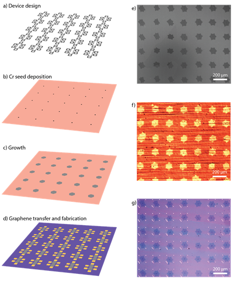

Image 1: (a)–(d) Proposed process flow for deterministic growth of single-crystal graphene. (e) Scanning electron microscopy (SEM) image of an array of graphene single-crystals. (f) Optical image of a graphene array on oxidised Cu foil. (g) Optical image of single-crystal array transferred on Si/SiO2 substrate with alignment markers. In figures (e)–(g) the array periodicity is 200 μm and crystal size is ~100 μm. Courtesy of 2D Materials
Large, single crystal graphene vs polycrystalline graphene
Single-crystal has various advantages over traditional polycrystalline graphene. While the grain size for polycrystalline graphene is 5-20 µm, single crystals can have a grain of up to 4cm, and while 95 percent of polycrystalline graphene is a monolayer, single crystal graphene allows a great deal of control over the thickness. Carrier mobility for single crystal graphene has been measured at RT 300 000 cm2/ Vs, higher than for polycrystalline graphene which is limited to 1000-3000 cm2/ Vs by the presence of grain boundaries. The positioning of the single crystals, however, is not controlled.

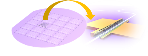
Image 2: Graphical depiction of the integration of graphene single-crystal arrays over wafers with wave guides. By Marco Giambra
Applications
The research team, a collaboration between IIT and CNIT, has demonstrated that it is possible to create graphene-based detectors and modulators with performance that is promising and indicate that graphene integrated photonics have the potential to solve present limitations.
The work has yielded detectors and modulators that demonstrate top performance for transmission and reception entirely through graphene devices, reaching world-record data rates for graphene devices (50 Gb/s for an electro-absorption modulator on SOI). Furthermore, the technology integrates at the back end of existent platforms. This, combined with the outstanding results for data transfer, have generated interest from data communications companies.
Applications for the technology include photonics, optoelectronics and electronics. The majority of the group's experience is in photonics, however. Graphene photonics applications are showing high level performance for the huge market of data center interconnectivity but also for urban and long-haul telecommunications.
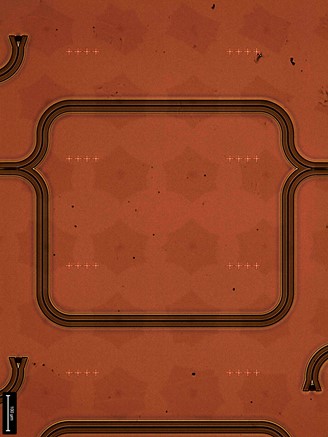
Image 3: Graphene arrays on photonic waveguides. By Vaidotas Miseikis
Collaboration yields success
The Graphene Flagship is a large-scale coordinated research initiative funded by the European Commission. Although their labs are close by, Coletti and Romagnoli never worked together until they both became partners of the Flagship and collaborations between their two work packages, one on enabling materials and another on wafer-scale system integration, brought them together. Continuous free exchange of personnel between their labs and common meetings combined expertise from material science (Coletti's lab) to device design (Romagnoli's lab), fabrication, testing, and packaging.
Other labs also contributed to the success by exploring other routes that provided useful suggestions to the CNIT-IIT work. In general, being part of a large project, like the Graphene Flagship, permits groups to collaborate with many partners and find the most appropriate path for each individual project.
Reference: Vaidotas Miseikis, Federica Bianco, Jé ré my David, Mauro Gemmi, Vittorio Pellegrini, Marco Romagnoli and Camilla Coletti. "Deterministic patterned growth of high-mobility large-crystal graphene: a path towards wafer scale integration." 2D Mater. 4 (2017) 021004
This article ran in the February 2019 issue of R&D magazine.
Author bio

Rebecca Waters
Rebecca Waters is Work Package Dissemination leader for the GrapheneEU project and the Dissemination Task Leader for the 2D Pilot Line. She oversees the Dissemination activities and manages the work package tasks and personnel. Rebecca also serves as the Graphene Flagship Communications Officer writing and disseminating news, managing the website and overseeing social media activities and media outreach. A former journalist with a degree from Northwestern University's Medill School of Journalism, Rebecca worked for both consumer and B2B magazines before joining the Graphene Flagship. In her spare time, she enjoys cooking, boating and exploring the world with her family.