


Spotlight: Miniaturising gas sensors for air quality monitoring
New technologies for the production of layered materials can help us manufacture low cost, chip-scale gas sensors for the Internet of Things (IoT).
Gas detection and air quality monitoring are important for our health, safety and wellbeing, so there is a critical need for gas sensors that are compact, low-cost and highly sensitive.
Arne Quellmalz is pursuing a Ph.D. at Graphene Flagship Associated Member KTH Royal Institute of Technology in Sweden under the supervision of Kristin B. Gylfason and Frank Niklaus. His research focuses on developing technologies to replace the current bulky and energy-consuming gas sensors.
In 2018, Quellmalz joined Graphene Flagship Partnering Project CO2-DETECT, funded by the FLAG-ERA Joint Transnational Call 2017, to work on the integration of graphene into air quality sensors. This project included researchers from Graphene Flagship Associated Members KTH Royal Institute of Technology and SenseAir AB in Sweden, Graphene Flagship Partners the Catalan Institute of Nanoscience and Nanotechnology (ICN2) in Spain, and AMO GmbH in Germany.
We talk with Quellmalz about his Ph.D. project on the integration of layered materials into semiconductor manufacturing lines and the recent developments in small and affordable air quality monitoring technologies. Quellmalz was awarded a grant from SCOPE – a coordination and support action that was funded by the European Commission between 2017 and 2020 for the benefit of the Graphene Flagship’s and Human Brain Project’s partnering environment – to attend Graphene Week 2019 in Helsinki. We take the opportunity to ask him about his experience at the biggest annual event of the Graphene Flagship.
How was your experience at Graphene Week 2019?
Graphene Week 2019 combined an excellent scientific program with the opportunity to get to know researchers and industry partners in the field. It was exciting to learn about the latest findings in layered material research, and I appreciated the direct discussion with fellow researchers. Their comments on our work were very valuable and helped me to steer my research efforts in the right direction.
What did you present there?
I presented our initial work on the transfer and integration of layered materials with conventional semiconductor substrates by adhesive wafer bonding. Earlier this year, we published these results in Nature Communications.
Graphene Week 2021 is approaching!
Have you thought about submitting a poster? The deadline is 31 July. All accepted posters are eligible for the best poster awards.
Can you tell us more about this new technique, and the benefits it will bring to sensors?
We employ tools, procedures and materials that are already well-established in the semiconductor industry. In this way, we can advance the development of miniaturized sensors with low production costs and power consumption.
If you want to build devices out of graphene or other layered materials, there is always a critical step: the transfer of the layered material from the substrate used to grow it to the final one on which you build the sensor. The transfer might cause wrinkles or cracks, which degrade graphene’s electric properties. In our approach, we obtain high-quality stacks of graphene and other layered materials, with the help of a standard dielectric resin. We use this resin like a glue, because it is solid at room temperature and viscous, like honey, at high temperature.
We create a sandwich by heating and pressing together a stack of the sensor substrate (silicon), the resin and the graphene sheet on its growth substrate (copper). At room temperature, the resin becomes solid and forms a stable connection between layered material and wafer. To stack more layers, we repeat the steps of heating and pressing. The resin becomes viscous again and behaves like a cushion, or a waterbed, which supports the layer stack and adapts to the surface of the layered material. This work was also part of the Graphene Flagship’s 2D Experimental Pilot Line (2D-EPL), which aims to bridge the gap between lab-scale manufacturing and large volume production of electronic devices based on layered materials.
In what way can graphene and layered materials improve these technologies?
Many gases, such as carbon dioxide and hydrocarbons (e.g. methane), absorb infrared (mid-IR) light, and one of the main components in these sensors are light detectors, which correlate light intensity to the concentration of a gas. Graphene and other layered materials are promising candidates to realise miniaturised photodetectors, because they absorb light very strongly and can be combined with semiconductor substrates.
Can you us more about the European research projects focused on air quality detection that you were a part of?
The Graphene Flagship Partnering Project CO2-DETECT is a collaboration between Graphene Flagship Partners Graphenea and ICN2 in Spain, AMO GmbH in Germany, Graphene Flagship Associated Members KTH Royal Institute of Technology and SenseAir AB in Sweden. This focused on the development of mid-IR detectors that can be integrated with silicon photonic circuits. By combining the theoretical and applied competencies of all partners, we demonstrated the feasibility of our concept and laid the groundwork for a follow-up project.
Why do you feel your research is important, and what benefits could it bring to society?
Cheaper, compact sensors could be used in mobile devices and wearables. They could be installed and distributed everywhere to report air quality in real-time, thereby provide valuable information about the air we breathe in everyday situations.
Air quality can vary severely from one street to another and decrease rapidly in closed spaces with poor ventilation. The information from our sensors could assist decisions on a personal level and, in the long run, help improve air quality and make people more aware of air pollution.
Our approach for integrating layered materials is generic and applicable to a broad range of areas, including photonics, sensing and neuromorphic computing. Since this employs only well-established processes and materials, we anticipate a low adoption barrier by industry. In the long run, it may speed up the creation of a new generation of devices that combine layered materials with traditional integrated circuits and microsystems.
What are the biggest milestones in your career – or your proudest moments?
The recent publication of our work in Nature Communications was a big milestone for me. I was very happy to see that it attracted a lot of attention in both academia and relevant industries, which indicates that we are trying to solve a relevant problem. This work was only possible thank to the great collaboration with Graphene Flagship Partners RWTH Aachen University in Denmark, the Universität der Bundeswehr München in Germany, AMO GmbH, and another company not yet affiliated to the Graphene Flagship, Protemics GmbH.
Why do you feel that diversity in science and technology is important for the Graphene Flagship's progress? What are you, your group or your institution doing to further this cause?
Solving problems and creating innovations are creative processes that often require a change of perspective to look at things from a different angle. I strongly believe that diversity is an advantage for every research group, since it can leverage the full potential of its members. My colleagues at the KTH Royal Institute of Technology are researchers from all over the globe, which I see as a strength of our institution.
What are your plans for the future?
We will continue working on the demonstration and validation of a full gas sensor system. It would be exciting to take on the next challenge and push this technology even further on the Technology Readiness Level, towards commercial use. Our industrial collaborators, which include Graphene Flagship Partner Graphenea in Spain and Graphene Flagship Associated Member SenseAir AB in Sweden, will be of great support for the next phase.
At the same time, we are investigating how to bring our integrated approach for the transfer and integration of layered materials to the industry. The outcome of this investigation is still open, but there may be an exciting endeavor ahead.
References
Quellmalz, Arne, et al. "Large-area integration of two-dimensional materials and their heterostructures by wafer bonding." Nature communications 12.1 (2021): 1-11.
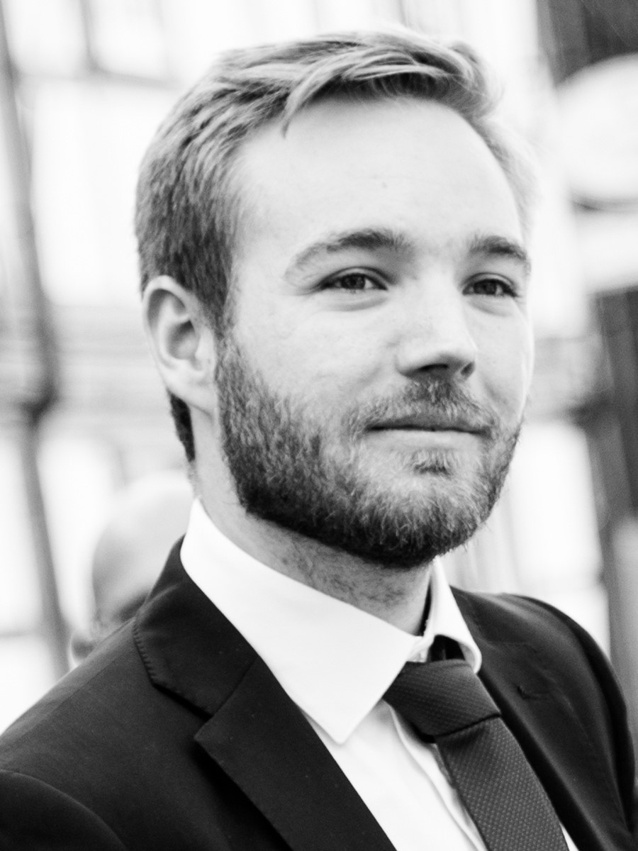
Quellmalz is developing technologies to replace commonplace bulky and energy-consuming gas sensors. Credit: Arne Quellmalz
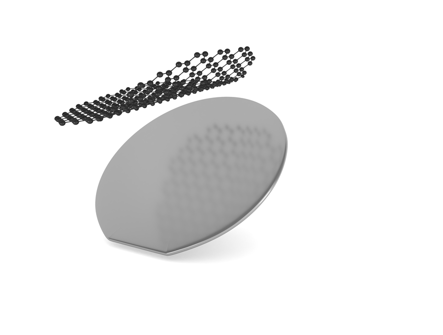
Schematic illustration of the transfer of graphene onto a wafer. Credit: Arne Quellmalz
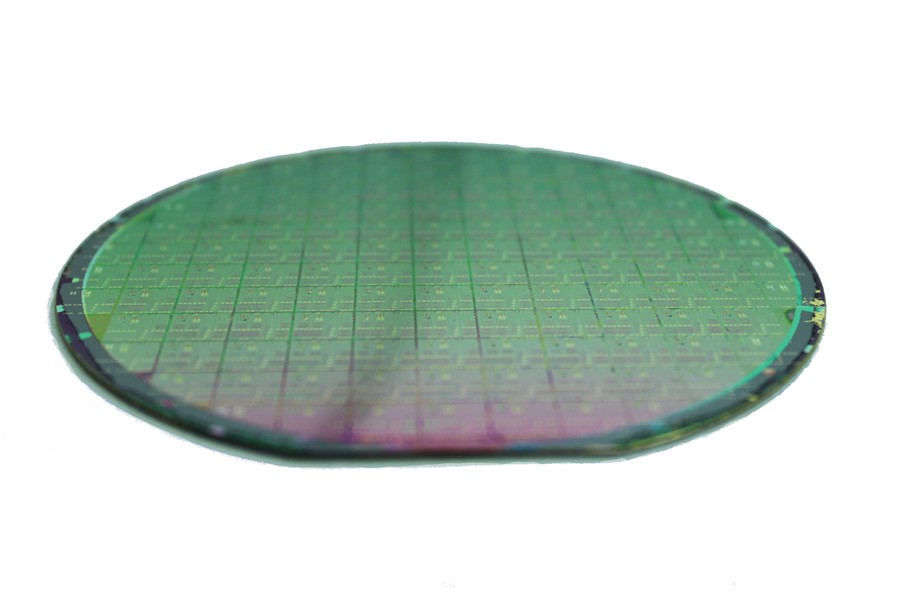
Photograph of a wafer with silicon photonic circuits and graphene photodetectors for optical gas sensing. Credit: Arne Quellmalz
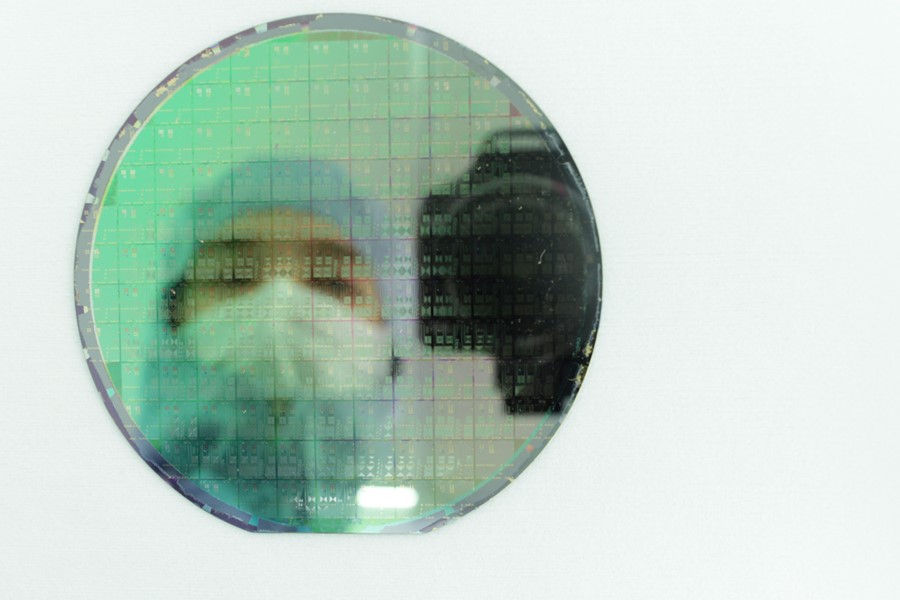
Quellmalz's reflection on a prototype wafer with optical gas sensors. Credit: Arne Quellmalz
Author bio

Letizia Diamante
Science Writer and Coordinator of the 'Diversity in Graphene' initiative.