
AMO electronic and sensor device platform

Overview
The AMO Electronic & Sensor Device Platform provides a robust prototyping environment for the fabrication of graphene and other two-dimensional (2D) material-based electronic and sensing devices. Built on AMO's extensive expertise in graphene integration on silicon technology, the platform enables researchers, startups, SMEs and industrial partners to accelerate the development of next-generation electronic and sensor solutions.
The platform combines advanced cleanroom processing, wafer-scale graphene integration and semiconductor manufacturing capabilities to deliver prototype devices suitable for research, validation and pre-industrial development.
Technology Platform
AMO has been developing graphene and 2D-material technologies since 2006, focusing on their integration with established silicon CMOS processes. The platform supports both electronic and sensing applications, leveraging the unique properties of graphene, including:
- High carrier mobility
- Ultra-thin device architectures
- Excellent sensitivity to environmental changes
- Compatibility with silicon-based technologies
- Potential for scalable wafer-level manufacturing
A baseline process for graphene device fabrication on 150mm/200mm silicon wafers is available and continuously improved. In the last MPW runs, process flows with bottom and/or top contacts, and local back gates were offered. The platform provides access to state-of-the-art semiconductor processing technologies, including:
- Wafer-scale graphene transfer
- Lithography and nanofabrication
- Graphene patterning
- Dielectric Deposition
- Metallization
- Device passivation
- Electrical test structure implementation
SPECIFICATIONS AT A GLANCE
- Different contact configurations available
- Carrier mobility is typically above 1000 cm2/V·s
- Minimum feature size (CD) ≈10µm, for both the graphene and the metal layers[1]
- Hall Bars, TLM devices, and field-effect transistors, available as a ready-made device library
- Individual device structures and process flows possible
ACCESS
This PDK is available free of charge to interested parties following the signature of a Design Kit License Agreement (DKLA) / Non-Disclosure Agreement (NDA). For more information or to request access to this PDK, please contact 2DPL@graphene-flagship.eu.
[1] A CD of 5 µm is also possible, but a detailed discussion is needed beforehand.
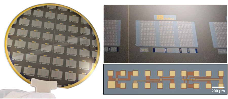
Wafer with dies and an optical micrograph of GFET, Hall bar and TLM structure.

About AMO
Located in Aachen, Germany, close to the borders of Belgium and the Netherlands, the research foundry AMO GmbH, a non-profit nanotechnology SME, follows the mission to efficiently close the gap between university research and industrial application. It demonstrates innovative technologies and introduces new materials, including their implementation in novel device architectures, prototyping and small volume fabrication. A state-of-the-art 400 m² cleanroom is operated and a range of services from consulting to prototype development is offered. In recent years, AMO has become a global player in 2D materials research for electronics and photonics.
AMO Gmbh
Otto Blumenthal-Str. 25
52074 Aachen
Germany
Email: 2d-PL@amo.de