
Process Design Kits

2D-PL Process Design Kits (PDKs) give you the building blocks, design rules and device models you need to turn innovative 2D material concepts into solid IC designs, to simulate physical data and realistic performances of next-generation devices.
Why 2D-PL PDKs?
MODEL 2D-MATERIALS BASED CIRCUITS
DESIGN WITH CONFIDENCE
Use defined design rules, layout guidelines and calibrated device libraries based on real process data to improve reproducibility and yield.
ACCELERATE DEVELOPMENT
Simulate and optimise circuits and integrated 2D material devices before fabrication, helping reduce development time, cost and risk.
BRIDGE R&D AND INDUSTRY
Evaluate new design approaches early and enable integration of 2D materials with existing technologies, including heterogeneous integration with CMOS.
Applications
PHOTONICS
Explore graphene-enabled photonic devices and integrated optical technologies.
SENSORS
Develop next-generation sensing technologies with tunable 2D material properties.
ELECTRONICS
Design and evaluate emerging Transition Metal Dichalcogenides-based electronic devices.
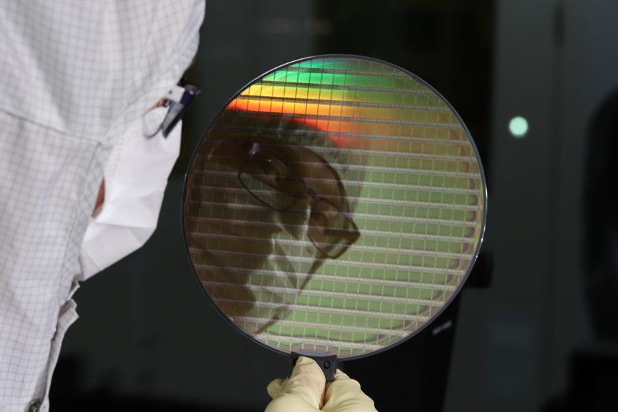
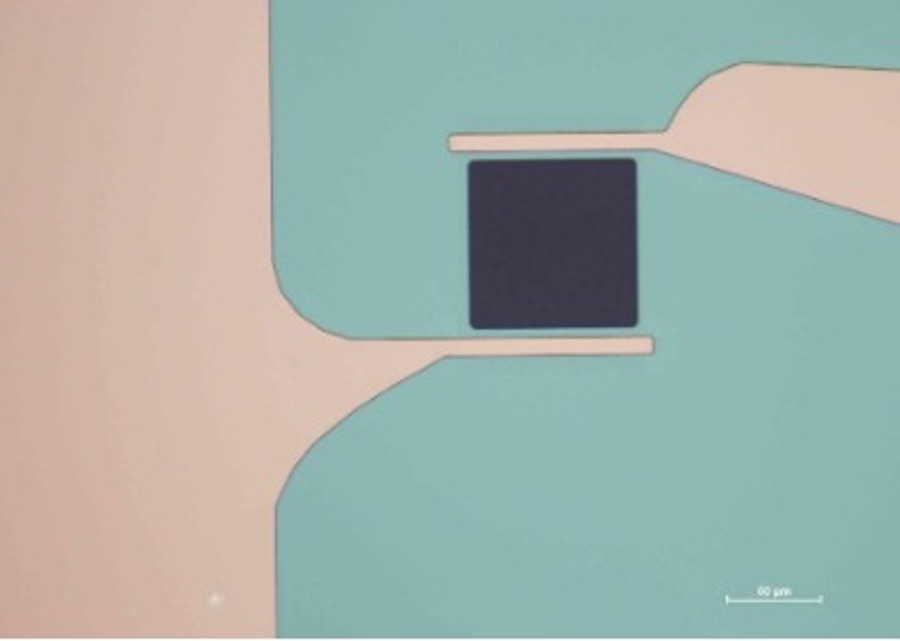
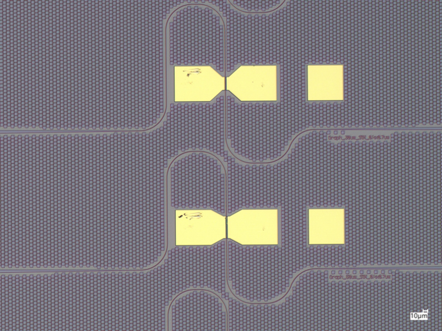
2D Pilot Line Process Design Kits


Hands-on PDK training on IC design and simulation of 2D materials-based photonic devices
Join us from 2–4 November 2026 for a three-day hands-on training on design practices for 2D material-based photonic integrated circuits (PICs) on KLayout. This course will guide participants from fundamental concepts and design tools to more advanced implementations and exercises for photonic device architectures using our 2D-PL partners’ four diverse PDKs. The event will be held at imec in Leuven, Belgium, and carried out by expert designers involved in the EU-funded project 2D-PL, a part of the Graphene Flagship initiative, and co-hosted by EUROPRACTICE.
