
Graphenea biosensing platform

The graphene solid-state device platform
At only one atom thick, graphene behaves unlike any conventional semiconductor. It supports device physics that silicon, germanium and other compound materials cannot reach, which is what makes graphene-based components worth exploring in the first place. Graphenea turns that potential into something you can actually build with: a route to prototyping and developing graphene-based solid-state devices for biosensing, optoelectronics and photonics.
The biosensing platform
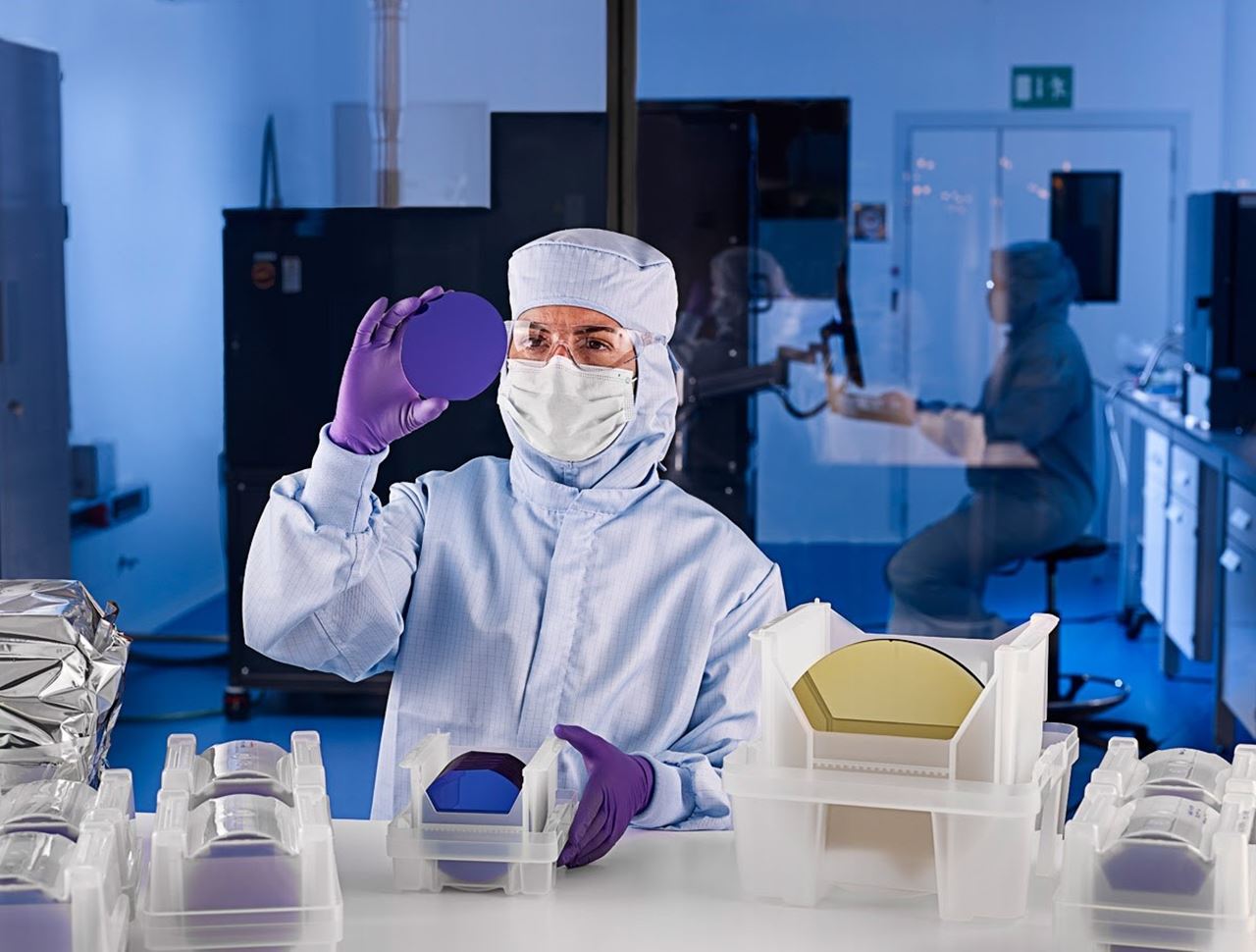
Rather than relying on exotic processes, Graphenea builds its graphene devices with the same wafer-scale manufacturing techniques used across the semiconductor industry. Two things follow from owning the fabrication process end-to-end. First, Graphenea can guarantee performance metrics on every run, so devices arrive meeting the customer's specification rather than a best effort. Second, because the manufacturing cycle is so much shorter than silicon's, it draws far less water, uses fewer process gases, and consumes less of the other chemicals and materials a longer process would require — which adds up to a meaningfully smaller carbon footprint per device.
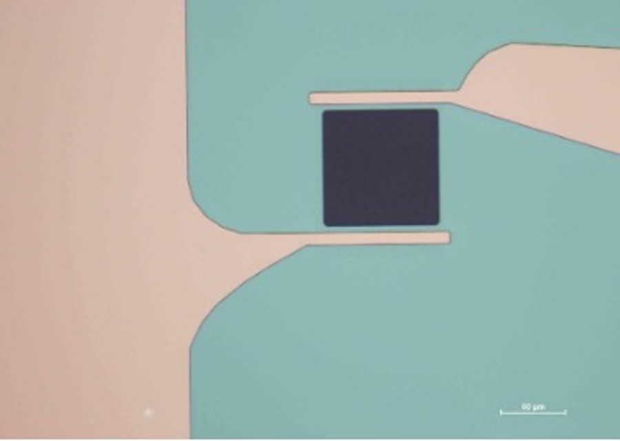
Graphenea established three process flows for the fabrication of several components such as resistors, capacitors, diodes, Hall sensors elements and field-effect transistors, or a combination of them on a single die.
Each process flow targets a different measurement environment: dry electrical sensing, wet biological sensing or gated, circuit-level devices. The design platform offered here focuses on process flow #2 dedicated to biosensing devices for liquid sample measurements. The platform runs on free, open-source CAD tools such as Klayout. There are device and cell examples, pads and die footprints that can be readily used for the design of a custom chip.
SPECIFICATIONS AT A GLANCE
- 2-, 3- and 4-terminal device architectures, selectable by process flow
- Carrier mobility typically above 1000 cm2/V·s
- Minimum feature size (CD) ≈10µm, for both the graphene and the metal layers
- Resistors, capacitors and field-effect transistors, available as a ready-made device library
BIOSENSORS
Process flow #2 operates in liquid environments. It is built for biosensing and liquid-biopsy work, where passivated contacts stop leakage currents and device degradation from creeping in on contact with a liquid analyte — so measurements can be taken directly in saline solution or in biological fluids like blood, plasma, saliva and sweat.
ACCESS
This PDK is available free of charge to interested parties following the signature of a Design Kit License Agreement (DKLA) / Non-Disclosure Agreement (NDA). For more information or to request access to this PDK, please contact 2DPL@graphene-flagship.eu.



About Graphenea Semiconductors
Graphenea, a technology company founded in 2010, is a world leading graphene producer. The 25 employees in Graphenea work on contributing to the successful development of graphene applications of our customers, in a wide range of sectors and in more than 60 countries in the world. Through research and innovation, we support our customers with our portfolio consisting of: CVD Graphene films, Graphene Field-Effect-Transistors chips (GFETs), Graphene Foundry Services (GFAB) and Graphene Oxides. Graphenea’s facilities are located in Spain (San Sebastián) and USA (Boston).
