
IHP photonics platform

Integrated graphene photonics
Graphene, with its unique electronic band structure, has the potential to enhance the functionality of a variety of devices. Despite advancements in the fabrication of graphene-based microelectronic devices, there are still issues with the stability and compatibility of integrating graphene devices with Si-technology processes. Therefore, it is crucial to investigate and prepare graphene devices in an environment that closely resembles Si technology. Towards these goals, IHP – Leibniz Institute for High Performance Microelectronics, focuses on the development of graphene integrated circuits in a 200 mm pilot line.
Integrated graphene photonics
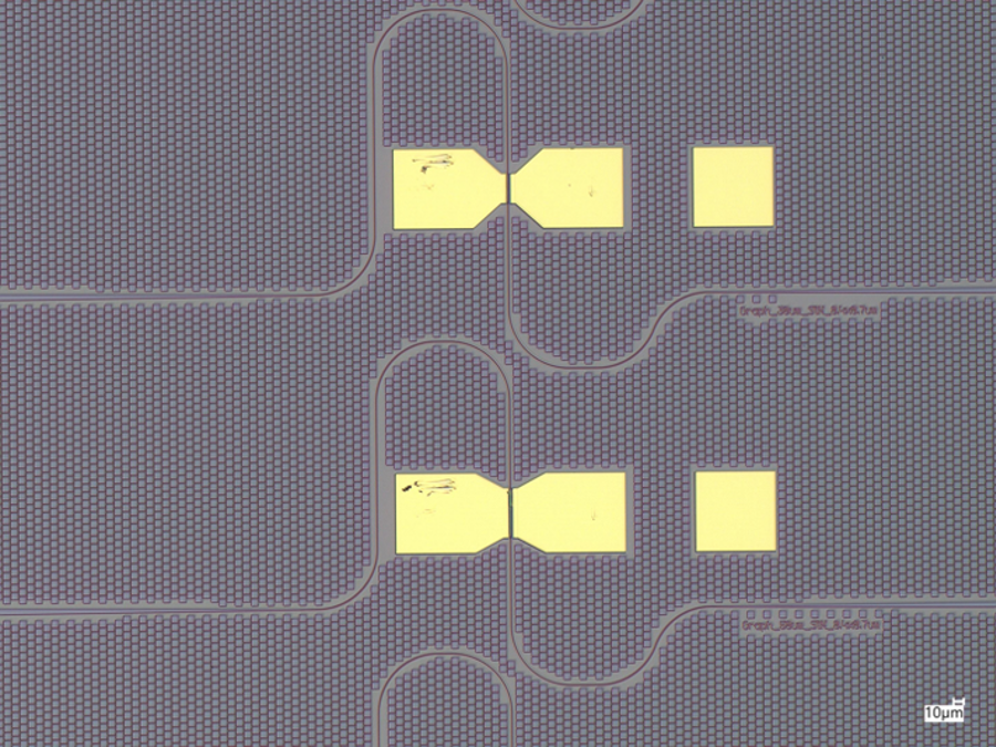
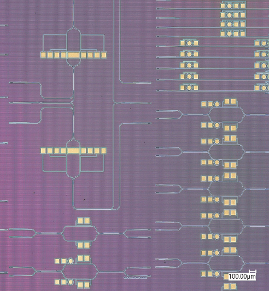
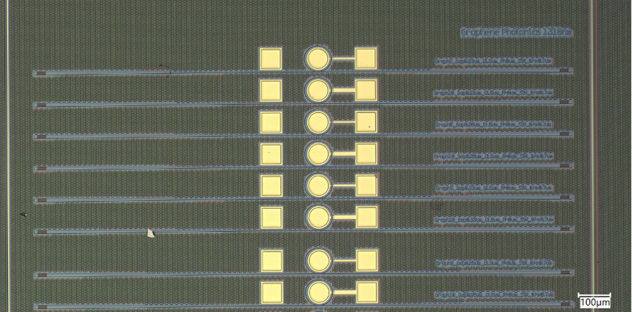
IHP is developing an integrated graphene photonics platform for the realisation of graphene-based photonic integrated circuits (PICs) on a 200 mm BiCMOS pilot line. The platform combines graphene devices with embedded SiN waveguides and explores scalable integration approaches for advanced photonic functionality. The dedicated process flow, based on a dual-layer graphene electro-absorption modulator (EAM), integrates essential contact, waveguide, and optical coupler modules with specialised graphene integration steps. Concurrently, cladding and encapsulation provide optical confinement and device protection. The incorporation of optional metal heaters allows for thermo-optic tuning and the addition of functionality. The process facilitates the fabrication and testing of various proof-of-concept devices, that are targeted for applications in high-speed optical communication, optical computing, sensing, and other emerging photonic systems. The associated Graphene Photonics Design Kit (PDK) provides a structured design-to-fabrication environment, including design and layout of fundamental photonic building blocks, system-level layout with filler structures, and layout verification using Design Rule Check (DRC) tools. Preliminary device libraries furnish experimental performance data for key components, including waveguides, grating couplers, and graphene modulators. The synergy of the 200 mm process technology, integrated device platform, component libraries, and PDK establishes a scalable workflow from photonic circuit design and verification to fabrication and experimental validation of graphene-enabled PICs.
ACCESS
This PDK is available free of charge to interested parties following the signature of a Design Kit License Agreement (DKLA) / Non-Disclosure Agreement (NDA). For more information or to request access to this PDK, please contact 2DPL@graphene-flagship.eu.
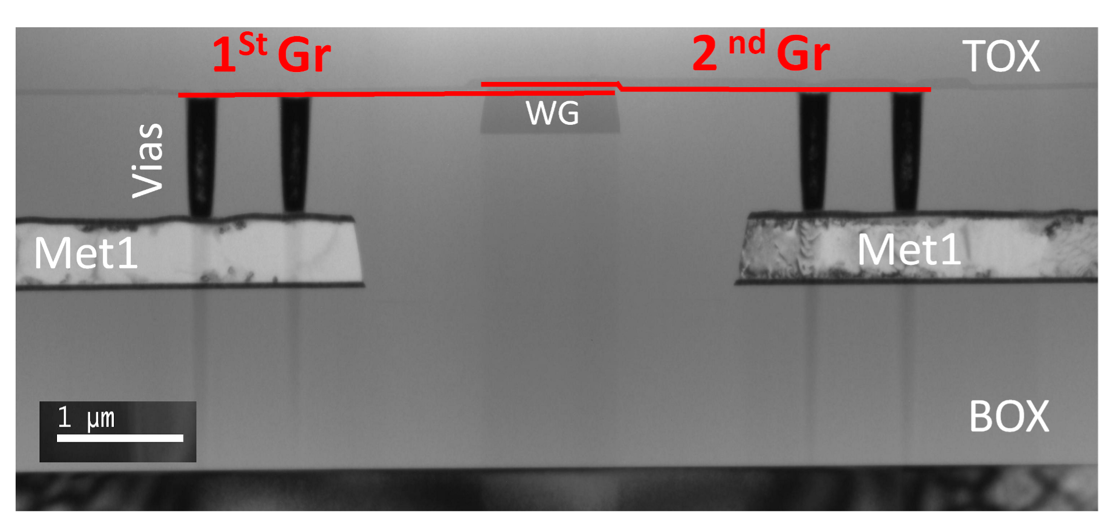
TEM cross section of dual layer graphene modulator on Si3N4 waveguide.
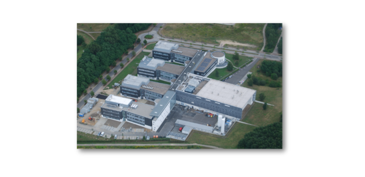
About IHP
IHP focuses on research and development in the field of microelectronics and information technology, in particular on the promotion of silicon-based high technologies to strengthen microelectronic research and industry in Germany and Europe. The spectrum of research work ranges from innovative materials to complex systems, e.g. for communication, which is a unique selling point in the research landscape. IHP covers the entire R&D value chain, from basic research to the manufacturing of prototypes and small series. The basis for IHP's capabilities is the institute's own continuously (24/7) operated pilot line with its qualified 0.25/0.13 µm SiGe BiCMOS technologies.
Currently, graphene, with its potential for functional extension of Si technology, is one of the research fields at IHP. The research includes material synthesis on 200 mm wafers in the IHP’s cleanroom and development of technological processes for graphene device fabrication in a 200 mm pilot line.
