
VTT CMOS integrated graphene-based devices

CMOS integrated graphene-based devices
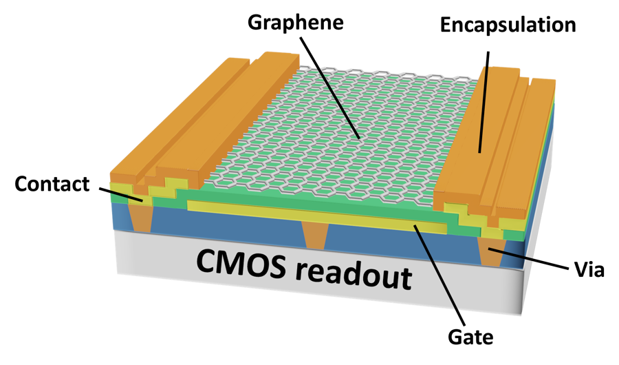
Graphene is an atomically thin material with extraordinary properties enabling next-generation devices and technologies. Its seamless integration with platforms such as CMOS BEOL enables enhanced functionality and efficient incorporation into existing semiconductor processes, paving the way for new innovations.
DESCRIPTION
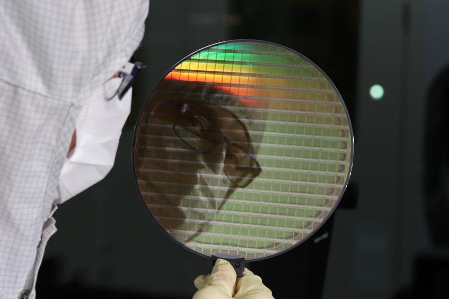
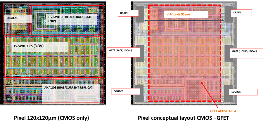
VTT uses commercially available Si CMOS readout wafers and standard semiconductor manufacturing techniques to produce CMOS integrated graphene-based devices at the wafer scale. The process flow enables graphene-based devices such as Field Effect transistors, resistors, and capacitors connected to the Si CMOS readout circuitry. VTT’s fabrication and quality control processes monitor key parameters in the runs, ensuring the customer’s devices are up to the targeted parameters. An example of the graphene FET CMOS integration by VTT is discussed in this publication.
KEY BENEFITS
- Enabling applications such as for e-noses, biosensor arrays, Hall sensors and IR cameras
- Large sensor arrays with multiplexing and integrated readout
KEY FEATURES
- 200 mm Si CMOS wafer
- X-FAB’s XH018 process for the Si CMOS readout
- 2D PDK plug-in compatible with XFAB’s XH018 PDK in Cadence
- DRC, LVS and simple device models available
ACCESS
This PDK is available free of charge to interested parties following the signature of a Design Kit License Agreement (DKLA) / Non-Disclosure Agreement (NDA). For more information or to request access to this PDK, please contact Senior Scientist, Miika Soikkeli (miika.soikkeli@vtt.fi).

About VTT
VTT Technical Research Centre of Finland Ltd is a state-owned non-profit research and technology organisation (RTO) with the aim of strengthening Finnish and European industrial competitiveness in multiple fields ranging from sustainable food and energy production to quantum computing. As an RTO VTT acts between universities and industry, bringing basic research towards industrial adaptation and helping the industry in their R&D needs. Graphene industrialisation at VTT is based on 2 600 m2 cleanroom in Micronova, Espoo, with a focus on wafer-scale CVD graphene process optimisation for electronics, photonics and sensors, including the integration on silicon CMOS for multiplexed sensor arrays. In addition to the MPW runs, VTT offers contract research, prototyping and small-scale manufacturing.