Jump to content

2D-EPL multi-project wafer run 1


EU Funded

This year the 2D-EPL project launched its first multi-project wafer (MPW) run where universities, research institutes and companies could include their designs as dies on joint wafers. The first run was mainly intended for graphene sensors, and was offered by AMO GmbH. 

What we offer:

  • Customizable chips
  • Short turn around
  • Flexible process flows
  • Direct communication channels
  • Experienced partners
  • Feasibility consulting

Important Dates

  • 1 February 2022: Call open, see specifications below
  • 30 June 2022: Call closes, design freeze
  • 1 September – 31 October 2022: MPW run

Pricing

  • 1300€ set price for four dies with identical design (1x1 cm²)
  • 250€ for each additional die with identical design 
  • 20% discount for customers from countries participating in the Horizon 2020 framework
  • Prices are exclusive of VAT, import duties/customs fees, withholding taxes, etc.
Two diagrams of graphene integrated on a device

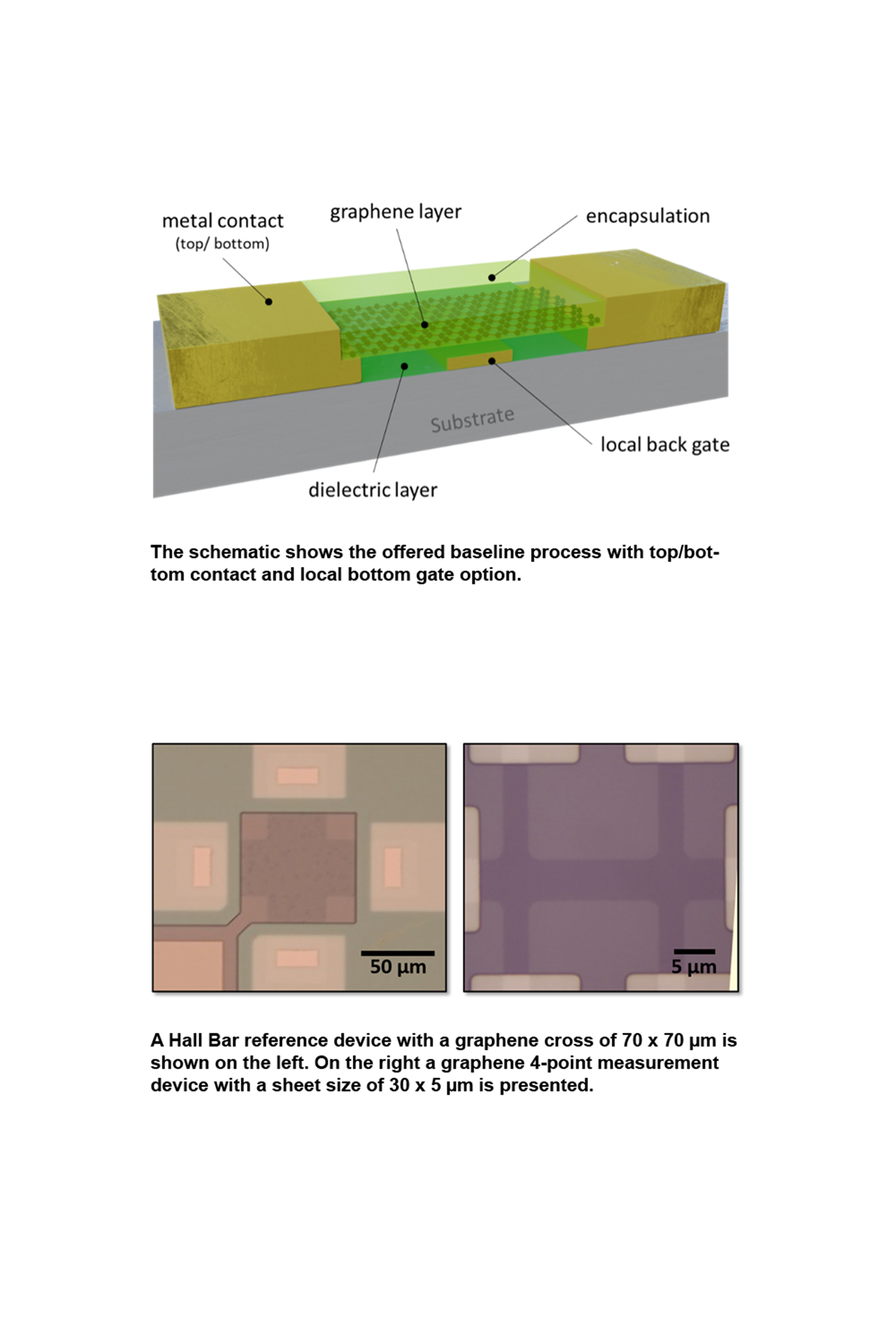
The offered baseline process for the first MPW run is a GFET including a top/bottom contact with an optional local or global back gate, an optional encapsulation and an optional graphene-area opening. The design of the device can be adjusted within the specifications listed below.

Specifications

Substrate

  • Material: Silicon, Glass
  • Basic die size: 1 x 1 cm² (a different size can be consulted upon individual request)

Resolution

  • General design rule: 5µm for in-layer critical dimension and over-layer alignment

Baseline Process

  • Top/Bottom metal contact
  • Wafer scale graphene transfer
  • Basic module provided in PDK: Hall cross, TLM devices, 4-point measurement bar
  • Optional: encapsulation, and via opening on top of metal pads
  • Optional: graphene sensing area opening
  • Optional: metal local or global back gate

Characterization

  • Optional: Raman characterization
  • Optional: Electrical measurement for as-fabricated devices

Application

  • Bio/ Gas/ Chemical sensors, Hall Sensors, Photodetectors
Learn more
Map or Europe with Aachen called out with an image of the AMO building

About AMO

Located in Aachen, Germany, close to the borders of Belgium and the Netherlands, the research foundry AMO GmbH, a non-profit nanotechnology SME, follows the mission to efficiently close the gap between university research and industrial application. It demonstrates innovative technologies and introduces new materials, including their implementation in novel device architectures, prototyping and small volume fabrication. A state-of-the-art 400 m² cleanroom is operated and a range of services from consulting to prototype development is offered. In recent years, AMO has become a global player in 2D materials research for electronics and photonics.