Ultra-thin logic: flexible computing with layered materials
Researchers from the Graphene Flagship have demonstrated the first fully functional microprocessor based on a layered material. The processor chip consists of 115 integrated transistors and is a first step toward ultra-thin, flexible logic devices.
The Graphene Flagship is developing novel technologies based on graphene and related materials (GRMs) such as transition metal dichalcogenides (TMDs), semiconductor materials that can be separated into ultra-thin sheets just a few atoms thick. Due to their thin, flexible nature and their excellent electrical properties at compact dimensions, GRMs are promising for compact and flexible electronic devices.
Researchers from the Graphene Flagship, working at the TU Vienna in Austria, have designed and fabricated the first microprocessors based on GRMs. Using transistors made from the TMD molybdenum disulphide (MoS2), the microprocessors are capable of 1-bit logic operations and the design is scalable to multi-bit operations. With the drive towards smart objects and the Internet of Things, the microprocessors hold promise for integrating computational power into everyday objects and surfaces.
Building Blocks of Computing
Microprocessors are a central part of modern electronics, from watches to smartphones and supercomputers. Based on transistors, logic operations are performed through a series of input and output cycles, according to instructions stored in a memory unit. Modern microprocessors are based almost exclusively on silicon, but this technology cannot be made flexible. The ultra-thin MoS2 transistors are inherently flexible and compact, so this result could be directly translated into fully flexible electronic devices, for example, wearable phones or computers, or for wider use in the Internet of Things. "In general, being a flexible material there are new opportunities for novel applications. One could combine these processor circuits with light emitters that could also be made with MoS2 to make flexible displays and e-paper, or integrate them for logic circuits in smart sensors," said Thomas Mueller, who led the work at TU Vienna.
The thinness of the MoS2 means that the transistors are highly responsive. "In principle, it's an advantage to have a thin material for a transistor. The thinner the material, the better the electrostatic control of the transistor channel, and the smaller the power consumption," said Mueller. The advantage of thin microprocessors means that low-powered computers could be integrated into everyday objects without adding bulk.
Complex Circuitry
The MoS2 microprocessor is the most advanced circuitry made with GRMs so far. The devices were tested using simple programs, delivering the correct results with excellent signal quality and low power consumption. Compared to modern processors, which can have billions of transistors in a single chip, the 115-transistor devices are very simple. However, it is a very early stage for a new technology, and the team have concrete plans for the next steps: "Our goal is to realise significantly larger circuits that can do much more in terms of useful operations. We want to make a full 8-bit design – or even more bits – on a single chip with smaller feature sizes," said Mueller. This goal presents a challenge in terms of design and fabrication: "Adding additional bits of course makes everything much more complicated. For example, adding just one bit will roughly double the complexity of the circuit," said Stefan Wachter, a researcher at TU Vienna and first author of the work.
Improving the multi-stage design process will be an important step in developing high-yield production methods for the MoS2 microprocessors, since – among other factors – the transfer of large area, bi-layer MoS2 onto wafers was a significant source of device failure. Dmitry Polyushkin of TU Vienna outlines the next steps: "Our approach is to improve the processing to a point where we can reliably make chips with a few tens of thousands of transistors. For example, growing directly onto the chip would avoid the transfer process, which would give higher yield so that we can go to more complex circuits."
Technology Horizons
Daniel Neumaier, from AMO, Germany, is the Leader of the Graphene Flagship Electronics and Photonics Integration Division, which aims to use the excellent properties of GRMs to enable new technologies in computing and telecommunications. "The transition from single devices to complex integrated circuits is a very critical milestone for the application of a specific technology, because it requires a high level of process control and reproducibility. This is a step towards the application of GRM-based electronic devices, especially in smart sensor systems and for flexible electronics," he said.
Silicon-based computing is a mature technology, and it is unlikely that GRMs will overtake silicon in the near future. However, achievements such as this demonstrate the potential for GRMs to enable new applications. "This simple circuit is a first conceptual step towards the implementation of simple logic in flexible devices for everyday use, such as food packaging or textiles," said Andrea Ferrari from the University of Cambridge, UK, the Science and Technology Officer of the Graphene Flagship, and Chair of its Management Panel. "The goal is not to compete head on with the established silicon technology, but to fill those complementary gaps not yet enabled by it."
Further Reading
S. Wachter, D. K. Polyushkin, O. Bethge, T. Mueller, Nature Communications 8, 14948 (2017)
Banner image: MoS2 transistors on the microprocessor chip, Hermann Detz, TU Vienna
The transition from single devices to complex integrated circuits is a very critical milestone for the application of a specific technology, because it requires a high level of process control and reproducibility."
Division Leader

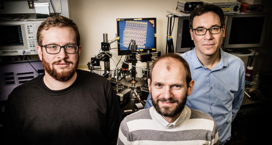
The research team at TU Vienna. Left to right: Stefan Wachter, Dmitry Polyushkin, Thomas Mueller. Credit: Marco Furchi, TU Vienna.


