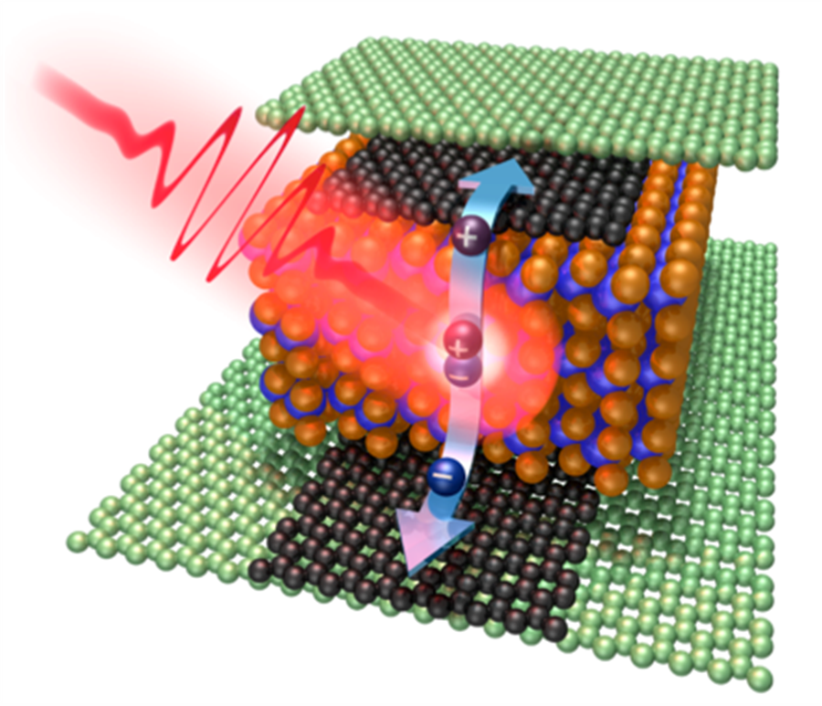
Graphene teams up with two-dimensional crystals for faster data communications
Ultra-fast detection of light lies at the heart of optical communication systems nowadays. Driven by the internet of things and 5G, data communication bandwidth is growing exponentially, thus requiring even faster optical detectors that can be integrated into photonic circuits.
In the recent work published today in Nature Nanotechnology, the research group led by Prof at ICFO Frank Koppens has shown that a two-dimensional crystal, combined with graphene, has the capability to detect optical pulses with a response faster than ten picoseconds, while maintaining a high efficiency. By using ultra-fast laser pulses, the researchers have shown a record-high photo-response speed for a heterostructure made of two-dimensional materials. These new materials are gaining more and more attention due to their amazing and rich variety of properties.
An important advantage of these devices based on graphene and other two-dimensional materials is that they can be integrated monolithically with silicon photonics enabling a new class of photonic integrated circuits. Although this study has been focused on the intrinsic properties of the photo-detection device, the next step is to develop prototype photonic circuitry and explore ways to improve large-scale production of these devices.
While Prof. Frank Koppens comments "It is remarkable how a material which is just a few nanometers thick can have such high performance", ICFO researcher Mathieu Massicotte and first author of this study states that "Everyone knew graphene could make ultrafast photodetectors, but related two-dimensional crystals were still lagging very much behind. In our work we show that by teaming up these two materials, we can obtain a photodetector that is not only ultrafast but also highly efficient."
The results obtained from this study have shown that the stacking of semiconducting 2D materials with graphene in heterostructures could lead to new, fast and efficient optoelectronic applications, such as high-speed integrated communication systems.
This study has been possible thanks to the support of the Fundacio Cellex Barcelona, the European Research Council (ERC) and the European Commission under the Graphene Flagship, among others.
Reference
Picosecond photoresponse in van der Waals heterostructures
M. Massicotte, P. Schmidt, F. Vialla, K. G. Schädler, A. Reserbat-Plantey, K. Watanabe, T. Taniguchi, K. J. Tielrooij and F. H. L. Koppens
Nature Nanotechnology
Link to the paper: http://dx.doi.org/10.1038/nnano.2015.227
More information
Research group led by Prof. at ICFO Frank Koppens
Contact Information:
Frank Koppens, ICFO

Image: graphene/WSe2 (2D material)/graphene heterostructure (© ICFO-Fabien Vialla)


