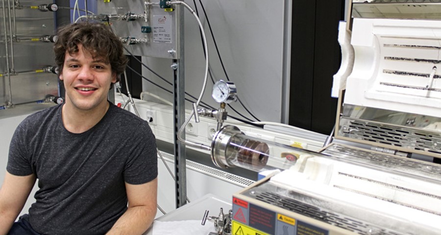
Spotlight: Luca Banszerus

In a new Spotlight series, the Graphene Flagship interviews promising early career researchers to highlight their contributions to excellent science across the Flagship. The first young researcher in the spotlight is Luca Banszerus, a PhD student in RWTH Aachen, Germany, working under the supervision of Christoph Stampfer.
Who do you want to see next in the Spotlight? Let us know at writer@graphene.cam.ac.uk!
Banszerus’s research on a dry-transfer of graphene grown by chemical vapour deposition (CVD) on copper has led to a simple and reliable transfer method. By allowing the interface between the graphene and the copper to oxidise, the adhesion between copper and graphene is weakened, and the graphene can be removed easily. This oxidation-assisted transfer process avoids the use of harsh chemicals to dissolve the copper, which also contaminate the graphene. The copper can be reused for further growth, with no change in the high quality of the CVD graphene. Banszerus is also the recipient of one of the Graphene Flagship’s Mobility Grants, and will travel to the US early next year to work with Philip Kim’s Low Dimensional Materials group in Harvard, MA. The Graphene Flagship asked Banszerus about his graphene research and future plans.
How did you get involved in graphene research?
During high school, I got involved in a science fair project on graphene together with another student who is currently also working in Christoph’s lab, Michael Schmitz. Graphene was heavily emerging at that point, in 2007. At first, we worked with exfoliation, and contacting tiny flakes with methods that are available in high school. Later on, we worked on larger samples from a simple, homebuilt CVD system. It was a quartz tube with a piece of copper on the inside, with pre-mixed gases flowing through and heated with a Bunsen burner.
That’s how I got involved with graphene, and also how I got to know Christoph, who was our mentor for the European level of the science fair competition. It is very beneficial if you are lucky enough to have a mentor who supports you in that way. In high school, we had our physics teacher; here I have Christoph, who really supports my work and gives me a lot of freedom in projects I can choose from, and also in every other way. It is important for the fun of it. That’s the main motivation, nobody would stay in the lab super long to work extra hours and push so hard if it wasn’t fun!
How did you develop the dry transfer process?
When we first started in Christoph’s group, we focused on growing graphene, and later on started to work on a dry transfer process. It was obvious that the contamination from polymers and ions originating from the transfer process is responsible for the low electronic quality that was observed in CVD graphene. We initially tried to pick up the as-grown graphene with exfoliated hexagonal boron nitride, which does not work very reproducibly. However, after letting the copper-graphene interface oxidise, the process works perfectly. Making use of the oxidation was more-or-less a lucky shot. We didn’t oxidise the graphene/copper interface on purpose, we just let it sit in ambient conditions for a few days. At one point, I just saw this oxidised graphene shape under the microscope – a flake where the graphene–copper interface had oxidised – so I thought “okay, let’s just give it a shot and see what happens”. It turned out that this worked far more reproducibly than without the oxidation, so in the end we were quite lucky.
What are you currently working on?
Now, we are working on different materials for the transfer, and also on scalable substrates for transferring. The method has so much potential, thus finding a way to scale it up would be extremely interesting. Additionally, combining CVD graphene with other 2D materials using the dry transfer process allows us to make use of the interesting physics in complex van-der-Waals heterostructures. I’m also doing a couple of side projects on Raman spectroscopy, quantum point contacts in molybdenum disulphide and on proximity induced superconductivity in graphene. One aspect that I would like to work on a bit more for my PhD is to combine more fundamental physics, with working on large area van-der-Waals heterostructures. One interesting example are interface effects, such as proximity-induced spin-orbit coupling, in graphene on a semiconducting transition metal dichaclcogenide (TMDC) material.
What are the next steps for your research?
In the US, the idea is for me to work heavily on technology. My personal goal is to just absorb as much new science and learn as much as possible. Philip Kim’s group is currently setting up an argon box cluster tool where one can make heterostructure samples from start to finish without the sample ever being exposed to water or oxygen. That’s equipment we don’t have here.
We are currently working on graphene-based heterostructures with semiconducting TMDCs like molybdenum disulphide and tungsten diselenide. The first benchmark would be to process these materials inside the argon box, and see what happens. Then one can go to more complex or air-sensitive 2D materials, for example, superconducting metallic TMDCs like niobium diselenide. The idea is to just characterise and see what’s possible.
Further Reading
1. L. Banszerus, M. Schmitz, S. Engels, J. Dauber, M. Oellers, F. Haupt, K. Watanabe, T. Taniguchi, B. Beschoten, C. Stampfer, Science Advances, 1, e1500222 (2015)
2. L. Banszerus, M. Schmitz, S. Engels, M. Goldsche, K. Watanabe, T. Taniguchi, B. Beschoten, C. Stampfer, Nano Letters, 16, 1387 (2016)
3. C. Neumann, S. Reichardt, P. Venezuela, M. Drögeler, L. Banszerus, M. Schmitz, K. Watanabe, T. Taniguchi, F. Mauri, B. Beschoten, S. V. Rotkin, C. Stampfer, Nature Communications, 6, 8429 (2015)
4. M. Drögeler, C. Franzen, F. Volmer, T. Pohlmann, L. Banszerus, M. Wolter, K. Watanabe, T. Taniguchi, C. Stampfer, B. Beschoten, Nano Letters, 16, 3533 (2016)


