


Fibre-optics data boost from graphene-based photodetectors
Research supported by the Graphene Flagship leads to fast, high-performance photodetectors for fibre-optic communication systems.
Optical fibres form the backbone of terrestrial and trans-oceanic telecommunications systems, and the huge volumes of data carried by these systems are limited by the ability with which photons can be registered as they pass through the cables. The same sensor technology is used in digital cameras, and in both cases the need is to record information efficiently and at high speed.
Infrared photodetectors in communications systems have traditionally been built as discrete devices connected to the optical fibre carrying the signal, and an electronic circuit for processing the received data. An improvement on this arrangement would be to integrate the detector and electronics on a single chip. This would substantially reduce the device footprint and fabrication cost.
The maximum data rate achieved with a state-of-the-art germanium detector fabricated using the standard silicon-based CMOS production system for integrated circuits is 40 gigabits per second. However, the performance of such photodetectors is limited by the material properties, and is less than optimal, owing to silicon’s vanishing light absorption at the wavelengths used. This is driving the search for new and better materials, and graphene is considered a promising candidate.
Graphene is crystalline carbon arranged in single atom-thick layers, with the carbon atoms set in a honeycomb-like lattice. This two-dimensional nanomaterial has a number of optical and electrical properties which give it huge potential for microelectronics and communications applications.
Schematic of an infrared photodetector with graphene as its active element (image: AMO GmbH)
In a paper recently published in the journal ACS Photonics, Daniel Schall and a team based at AMO in Aachen, and Alcatel-Lucent Bell Labs in Stuttgart, demonstrate photodetectors based on wafer-scale graphene. The devices are capable of recording data at up to 50 gigabits per second, and display excellent signal integrity.
Study leader Daniel Schall is a 32-year-old electrical engineer who has been with AMO since 2009, and is currently working toward a PhD at RWTH Aachen University. His work on graphene is supported by the European Commission through the Graphene Flagship, and the ACS Photonics paper on graphene-based photodetectors is the highlight of the journal issue in which it is published.
The Graphene Flagship is the world’s premier research initiative devoted to graphene and related two-dimensional nanomaterials. It is a visionary, science-driven academic-industrial partnership bringing together scientists and engineers from across various European countries and technical disciplines. Underpinning the Graphene Flagship is a single-minded focus on a disruptive technology set to have a massive impact on human society.
Graphene is of special interest as a material for photodetectors owing to its light absorption across the electromagnetic spectrum from far-infrared to ultraviolet, and high electric charge carrier mobility. Graphene-based photodetectors are also free of the residual electric current that can beset opto-electronic devices when no photons are present.
Commenting on the advantages of graphene, Schall says: “Graphene has outstanding properties when it comes to the mobility of its electric charge carriers, and this influences the speed at which electronic devices operate.” Environmental infrared sensors, such as those designed to detect the presence of gases, are also conceivable with graphene, he adds.
When it comes to device fabrication, graphene can be integrated with silicon substrates at the wafer scale. This makes graphene a very attractive material for electronics engineers.
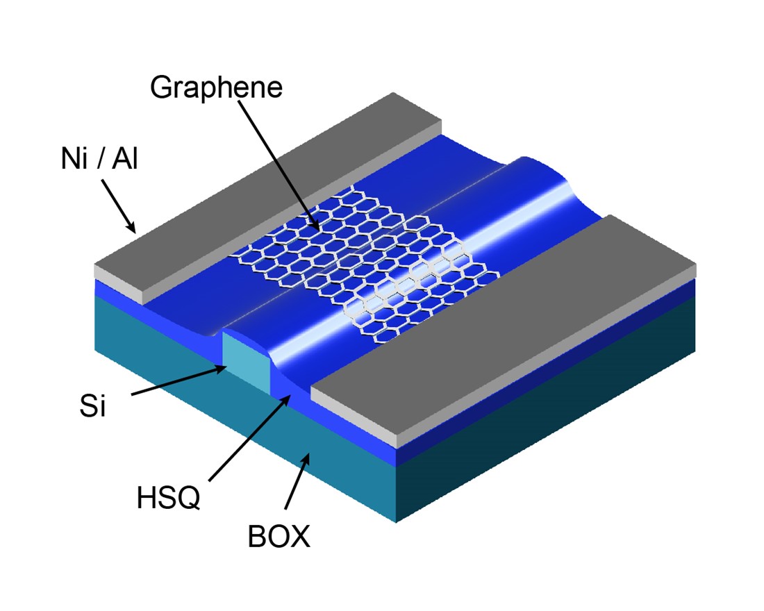
The AMO and Alacatel-Lucent photodetector is made up of a base on top of which lies a 400-nanometre-wide silicon strip electromagnetic waveguide overlaid with a graphene layer set between nickel and aluminium contacts. The graphene is deposited on the substrate from a vapour, and protected from cracking at the step edges of the waveguide with a spin-coated layer of an organic-silicon compound known as HSQ.
Science aside, Schall stresses that AMO’s ongoing work on graphene-based photodetectors will cover the entire device fabrication process from laboratory to factory floor. “We benefit greatly from our existing production platform and the related technology,” he adds. “For the next generation devices, we are looking for a data rate in the 100+ gigabit per second regime.” Schall and his colleagues are also working to improve the sensitivity of their devices.
Integrating graphene-based photodetectors into the universal CMOS production system for integrated circuits will allow for the development of entire photodetection systems.

Graphene has outstanding properties when it comes to the mobility of its electric charge carriers, and this influences the speed at which electronic devices operate.”
Researcher AMO GmbH