


Graphene Week 2015 – science highlights from day 1
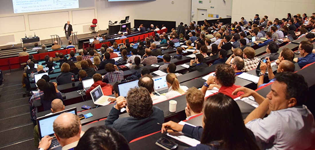
In a previous article, we looked at keynote presentations from the first day of Graphene Week 2015 in Manchester. Here we outline the contributed science talks from the first day of the conference, of which there were nine in each of two parallel sessions.
Fundamental science of graphene and related materials
The first of two parallel sessions on Monday afternoon was given to the fundamental science of graphene and related 2d materials.
Dong-Keun Ki from the University of Geneva discussed the even-odd effect of interactions in Bernal stacked graphene multilayers. Ki and his colleagues have studied how electrical conductivity in graphene varies with the number of stacked layers, and found that an even number of layers leads to insulating behaviour. Odd-number layers remain conducting at low temperature.
Tokyo University’s Satoru Masubuchi spoke of magneto-transport effects in slightly twisted bilayer graphene. Observations show that bilayer graphene with small twist angles constitutes a new type of 2d electron system which differs from both monolayer graphene, with its square-root dependence of energy with magnetic field, and Bernal stacked bilayers.
Continuing with the stacking theme, Petr Stepanov from the University of California Riverside discussed the quantum Hall effect in ABA-stacked trilayer graphene. Stepanov and his colleagues found that this form of graphene provides an excellent platform for pseudo-spin physics. Landau-level crossing is observed, and this can be explained in the context of a single particle picture in tight binding calculations.
Manchester-based Artem Mishchenko has been studying valley currents, pseudo-spin and chirality in Dirac materials such as graphene. He showed how changing pseudo-spin in monolayer and bilayer graphene leads to valley currents, and discussed chirality conservation in resonant tunnelling transistors constructed from crystallographically-aligned graphene layers separated by monolayer hexagonal boron nitride.
Aalto University’s Pertti Hakonen and his colleagues are working on electron-phonon coupling in suspended mono- and bilayer graphene. This is relevant to the control of energy transport in a variety of devices, sensors included. Hakonen reported that flexural modes are very important in monolayer graphene.
Leonardo Vicarelli from Delft University of Technology discussed in-situ electrical measurements of graphene nanoribbons. Vicarelli and his colleagues have performed electrical measurements of graphene using in-situ scanning transmission electron microscopy, and observed band-gap opening and edge shape dependence in sculpted graphene.
Regensburg University researcher Jonathan Eroms discussed ballistic transport in graphene antidot arrays, focusing on observations of magnetoresistance peaks in monolayer graphene. Boron nitride-encapsulated graphene was found to display very high mobility.
Manchester’s Ivan Marun reported on the direct measurement of Peltier cooling and heating in graphene, which arises when an electric current passes across a junction between two materials. With a specialised thermoelectric architecture, the researchers have carried out the first direct electrical detection of the Peltier effect in graphene.
Madrid-based researcher Guillermo Lopez-Polin spoke next of the influence of thermal fluctuations on the mechanical properties of graphene. He showed how defects can double the material’s elastic modulus and quench thermal fluctuations. Thermal contraction decreases with defect density, whilst elastic modulus increases with strain.
Production of graphene and related 2d materials
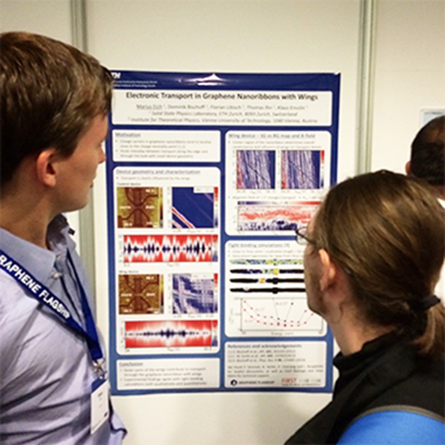
Following the oral presentations was a poster session sponsored by Texas Instruments
The second parallel session on Monday afternoon was devoted to graphene production.
Gui-Ping Dai from Nanchang University looked at selective chemical vapour deposition of graphene for device applications. Dai and his colleagues have studied square-shaped monolayer graphene domains, and observed that grains can retain their shape across curved copper substrate boundaries.
Siamak Nakhaie from the Paul-Drude Institute in Berlin spoke of the synthesis of hexagonal boron nitride films on nickel foils by molecular beam epitaxy. Dendritic, star-shaped BN islands are seen, moving to smooth-edged triangles with an increase in process temperature.
Continuing with the boron-nitride theme, UK National Physical Laboratory researcher Barry Brennan discussed nucleation control for large single-crystal domains of hBN via silicon-doped iron catalysts. Structures with sizes of around 300 microns are seen. Silicon promotes crystal growth, and stabilises the hBN monolayers.
Sukanya Dhar from the Indian Institute of Science in Bangalore illustrated a predictive approach to the growth of molybdenum disulphide monolayers by “true” chemical vapour deposition. The intent is to develop a method in which the precursors are vaporised from sources outside the CVD vessel, but without the uncontrolled growth that typically results from the high pressures and large driving forces involved.
Timothy Booth from Denmark’s Technical University in Lyngby discussed the production of graphene from recyclable thin-film catalysts with improved field-effect mobility over that from established techniques. Booth showed that high-quality graphene can be produced using relatively small quantities of copper catalyst, which can then be re-used whilst preserving the graphene quality.
A tug-of-war between corrugation and binding energy was described by Carlos Romero-Muñiz from Madrid. Such a battle can seen in the formation of multiple Moiré patterns on a strongly interacting graphene-metal system. The results are especially important in fine-tuning the electrical properties of graphene via substrate interactions.
Tom Yager from Chalmers University in Göteborg outlined the fabrication of high-mobility epitaxial monolayer graphene devices via aqueous-ozone processing. The observed transition from strong n-type doping to low p-type can be explained as the result of processing and annealing, as the removal of resist residuals exposes the bare graphene to dopants present in ambient conditions.
The functionalisation of graphene nanoribbons, and the influence of edges and intercalates on transport characteristics, was discussed by Christoph Tegenkamp from Leibniz University in Hannover. NPN-type structures with Klein tunnelling barriers have been realised by functionalising the buffer layer on top of silicon carbide mesas via germanium intercalation.
The final talk of the session was given by Matthias Mecklenburg from the Technical University of Berlin. Mecklenburg presented an overview of aerographite, a synthetic foam made up of interconnected graphite tubes. He also looked at how the CVD process can be tuned for aerographite in various applications.
Posters on fundamental science and graphene production
Following the oral presentations was a poster session sponsored by Texas Instruments. Eighty-five posters covering fundamental science and graphene production were on display, with the lead authors present to discuss their work with interested onlookers.
Photos: copyright © 2015 Anders Frick, Chalmers University of Technology