


Switched On: Designing High-Performance Waveguide Switches and Modulators with Graphene
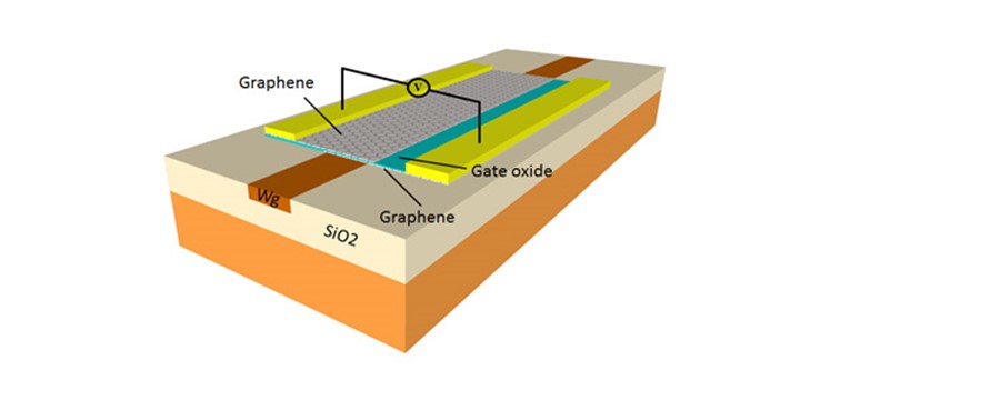
Design for a graphene-based silicon waveguide modulator or switch using two layers of graphene. Illustration by Leili Shiramin, Ghent University.
Researchers from the Graphene Flagship have explored the design principles for integrating graphene with silicon and silicon nitride waveguides to form high performance switches and modulators. These devices will play a key role in new telecommunications technologies.
To meet ever-increasing demands on speed and capacity, telecommunications networks must keep ahead using innovations in research and technology. In the near future, graphene-based devices are expected to play a key role in communications and networking, enabling high-speed and high-capacity infrastructures.
In such devices, enhancing the coupling between the graphene components and optical signals is crucial to achieving efficient graphene-based optoelectronics and photonics. One promising method of improving coupling is integrating graphene devices with waveguides. As part of the Graphene Flagship’s aims to bring graphene-based technologies into real-world applications, researchers at IMEC in Belgium have explored the optimum configurations for graphene–waveguide coupling devices acting as switches and modulators. Published in the IEEE Journal of Selected Topics in Quantum Electronics, these results provide clear guidance for careful design of graphene-based optoelectronic switches and modulators, which will be cornerstones of graphene-based optoelectronics networks.
Optoelectronics is an area where graphene is making a significant impact. The unique optical and electronic properties of graphene open up exciting possibilities for interfaces between light and electronics for a range of applications including security, sensors, and displays. The Graphene Flagship is achieving great strides in communications research, with lower power consumption and faster data transmission and processing promised in the integration of graphene technologies with industry-standard telecommunications. Professor Frank Koppens, of ICFO, Spain, who leads Work Package 8 – Optoelectronics and Photonics says “Graphene offers an all-in-one solution for data communications applications, particularly in low-cost integrated Si photonics. This is because of its gate-tunable optical properties, ultra-fast response time, spectrally broadband operation and compatibility with Si-CMOS and SiN photonics. Therefore, graphene allows for a monolithic integration of phase and absorption modulators, switches and photodetectors, with higher performance, high speed and smaller footprint. Within the Work Package, we are also developing broadband photodetectors for visible, IR and THz, with performances beyond the state of the art, as well as the first photodetection arrays, integrated with CMOS electronics or flexible platforms.”
For telecommunications applications, the details of the trade-offs between speed, bandwidth, device size, losses, and materials are crucial for efficient operation. In the article, four different device configurations based on either single- or double-layer graphene integrated with silicon or silicon nitride waveguides are examined. The silicon and silicon nitride waveguides studied are well-used in telecommunications applications, and the devices are assessed at optical telecommunications wavelengths of 1310 and 1550 nm. While silicon waveguides allow for smaller devices, the silicon nitride fabrication process is more configurable. Graphene layers can be embedded directly inside a silicon nitride waveguide, providing increased graphene–light interaction, and these devices could potentially be incorporated into larger heterostructures.
The researchers found that in static operation – i.e. switching – the overall performance does not depend on the particular device configuration, but instead on the purity of the graphene and the thickness of the insulating layer of aluminium oxide between the graphene layers. In both static and dynamic operation, the most important factor is the aluminium oxide thickness, with a thicker layer decreasing modulation efficiency and increasing operation voltage and power consumption, but extending modulation bandwidth.
For dynamic operation as a modulator, this research indicates that the key parameters affecting the modulation bandwidth are the device dimensions. Due to the increased confinement of the waveguide compared to the silicon nitride devices, the silicon waveguide allows for faster modulation of up to 25 GBit/s over a wide modulation bandwidth of 16 GHz. On the other hand, a similar silicon nitride device provides an excellent switch, with fast switching time of 0.4 ns and large on/off ratio of 23 dB.
Professor Dries Van Thourhout, from IMEC, Belgium, one of the authors of the paper, describes the motivation for the study: “One of the aims of Work Package 8 is to develop graphene based integrated modulators, switches and detectors for next generation telecom and data communications networks. We have evaluated the theoretical performance of double layer graphene based modulators and switches, and provided some guidelines for their practical realisation. Once initial prototypes are demonstrated it is important they get packaged and tested in real-world conditions.” This research provides a solid foundation from which to evaluate performance of graphene–waveguide devices, and design devices according to specific applications.
In order to realise graphene-based switches and modulators and similar devices, precise fabrication techniques are required. Professor van Thourhout explains the next steps: “Basic devices using standard CVD-based graphene have been realised. To reach ultimate performance the fabrication needs to be improved by reducing the background losses and reaching sufficiently thin layers of high quality graphene. Several Graphene Flagship partners are currently developing the critical processing steps needed to realise these devices, as well as ways to transfer these fabrication processes to large-scale CMOS facilities.”
Professor Marco Romagnoli, of CNIT, Italy leads Work Package 10 – Wafer Scale Integration, and is coordinating the development of large-scale production and integration with silicon and other wafer technologies to enable industrial manufacture: “Solutions for large scale production are important to transform a handcraft approach into an industrial model. The challenge is to implement all required steps with techniques that preserve the performance of graphene.” A key advantage of graphene is its ability to be integrated directly with existing silicon microelectronics. “The combination of the excellent properties of graphene with the integrability with CMOS processes makes graphene technology a unique opportunity for the future evolution of low cost, low consumption and large bandwidth photonics,” he adds. An important target of Work Package 10 is the development of a fully-compatible fabrication process for producing graphene-based modulators on full scale silicon wafers.
Professor Andrea Ferrari from the University of Cambridge, UK, is Chair of the Flagship Management Panel, and its Science and Technology Officer. He states that "This work is one of the steps necessary to fulfil the potential of graphene in photonics and optoelectronics. The partnership with IMEC is instrumental for the flagship to reach the ambitious goal to translate these predictions into real and scalable devices by mid-2018." Across the Graphene Flagship, research is underway to improve fabrication compatibility and scaling, to provide all the necessary ingredients to take graphene technologies from research directly into real-world situations.
Further Reading
L. A. Shiramin, D. Van Thourhout, IEEE Selected Topics in Quantum Electronics, 2016 DOI: 10.1109/JSTQE.2016.2586458
V. Sorianello, M. Midrio, M. Romagnoli, Optics Express, 2015, 23, 6478
M. Midrio, P. Galli, M. Romagnoli, L. C. Kimerling, J. Michel, Photonics Research, 2014, 2, A34
M. Midrio, S. Boscolo, M. Moresco, M. Romagnoli, C. De Angelis, A. Locatelli, A.-D. Capobianco, Optics Express, 2012, 20, 23144
The combination of the excellent properties of graphene with the integrability with CMOS processes makes graphene technology a unique opportunity for the future evolution of low cost, low consumption and large bandwidth photonics."
Work Package Leader