2D-EPL: Wafer scale integration

The work done in the 2D Experimental Pilot Line’s (2D-EPL) Wafer Scale Integration Work Package will develop the processing steps needed for the fabrication of graphene and other 2D material-based devices, such as field effect transistors. This includes the optimisation of the material patterning, contacting and passivation from the environmental effects. A significant effort is also being placed on quality control development to ensure high stability and quality of the devices.
This year’s progress
The definition of quality control protocols has been an important step during the first year of the 2D-EPL. Our work package has established common key control characteristics and protocols to enable all project partners to provide clear and transparent comparison and reporting. The work was done in collaboration with Graphene Flagship’s standardization committee and the International Electrotechnical Commission (IEC) to move forward with the standardisation of the protocols.
The biggest technological accomplishments this year were the demonstration of TMDC based transistors on 300 mm wafers and GFETs integrated with a CMOS readout on 200 mm wafers. The scientific accomplishments include advances in the interface optimisation between graphene and Si wafer substrates and dielectric deposition on graphene and TMDC layers.

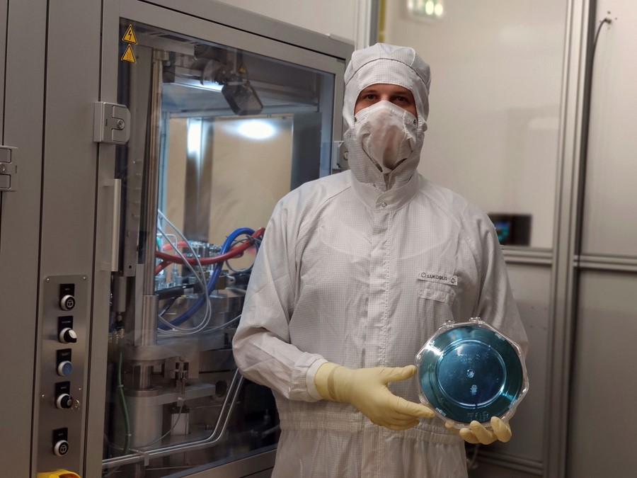
Work package deputy, Mindaugas Lukosius, works in the IHP cleanroom. Credit: IHP
Collaboration
Partners are well connected across 2D-EPL and Core 3 work packages. Inside the 2D-EPL GSEMI provides graphene on 150 mm and 200 mm wafers to AMO and VTT, and micro resist technology in the Wafer Scale Transfer work package is developing custom resist to be utilised for graphene patterning in our work package. AMO and imec also work in the Wafer-scale System Integration Work Package of the Core 3 project. VTT is utilizing the processes developed by our work package to enhance the graphene field effect transistor integration efforts in the Core 3 Sensors Work Package and the GBIRCAM spearhead project. imec is also part of the Autovision and METROGRAPH spearhead projects which benefit from our development efforts.
What’s in store
The processes developed by our work package are intended for use in the multi-project wafer (MPW) runs, which will launch in 2022. They will also be made available directly to the pilot line partners. The partners have already established stable process flows in the pilot line sites that can be utilised in the product development for customers, bringing our technologies directly to industry. The first MPW runs will focus on providing services for companies interested in graphene-based sensors. Further process optimisation, in the coming years, will enable higher electrical quality of the devices in the future. The later MPW runs will include electronics and the integration of devices on top of CMOS readout wafers.
The main technological challenges for our work package are in achieving stable processes with high electrical quality in the key control characteristics such as mobility, contact resistance, doping and hysteresis. This work includes precise optimisation of the full process flow including interfaces, dielectrics, contacts and passivation. The development of the 2D material specific processing steps is crucial to ensure devices with high electrical quality because even high-quality material growth and transfer is easily hindered by suboptimal process flows.
The processes developed by our work package are intended for use in the multi-project wafer (MPW) runs, which will launch in 2022. They will also be made available directly to the pilot line partners.
Work Package Leader
