Wafer-scale System Integration
Graphene meets silicon wafers
The aim of the Wafer-scale Integration Work Package is to bring graphene integration maturity from the laboratory to semiconductor manufacturing plants, or “fabs”.
The last 10 years
The incorporation of graphene into electronic and photonic components can enhance their performance in terms of size, power and energy efficiency. It is also the next step to enabling graphene-based commercial products. However, integrating graphene into mature manufacturing processes within the semiconductor industry is not an easy undertaking.
The Work Package was established in Core 1 to address the integration challenges that hindered the successful implementation of graphene in industry, mainly focussing on the manufacture of electronic and photonic integrated devices. Over the course of eight years, the Work Package has made significant progress in improving the manufacturing and fabrication of graphene materials (including steps such as contacting, patterning and encapsulation). Efforts have also been made to enhance the wafers’ scale, which increased from 50 mm up to 200 mm, and the quality of graphene.
One of the great advantages of the Graphene Flagship for our Work Package has been the long-term collaborations between research institutes, universities and companies. This has enabled tremendous progress in our work. Through collaboration, researchers from academia and industry have been able to tackle and solve relevant problems and ultimately move one step closer to graphene industrialisation. It also built a European ecosystem around graphene and layered materials.
Last year’s progress
The Wafer-scale Integration Work Package’s efforts focused on Hall sensors as electronic components and electro-absorption modulators as photonic components.
In 2022, the researchers transferred 200 mm CVD graphene on a 300 mm waveguide containing wafers in imec’s 300 mm CMOS platform, achieving high uniformity and yield. The process met the semiconductor industry's metal contamination requirements for back-end-of-line, with a concentration of iron and copper contaminants lower than 1012 atoms/cm2 on 200 mm CVD graphene. Additionally, CVD graphene deposited on various substrates, such as aluminium oxide and silicon dioxide, showed improved charge carrier mobility values of 10,000 cm2/Vs.
Furthermore, the Work Package has developed graphene-enabled electro-absorption modulators with data-rate of 20 Gbps and high-speed photodetectors with data-rate up to 120 Gbps. These advances demonstrate the potential for energy-efficient photonic components using graphene technology.
Amaia Zurutuza, Work Package Leader
Europe can now demonstrate graphene-based wafer-scale photonic and electronic components, something that ten years ago was truly out of reach.”
Work Package Leader
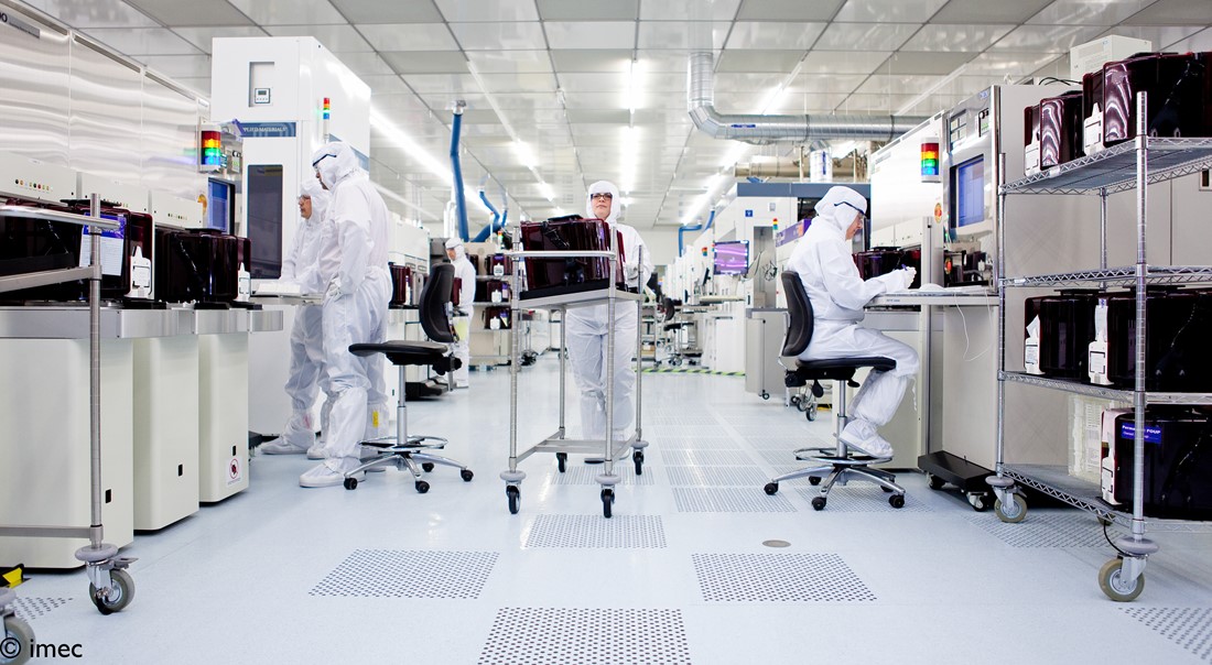
A look inside imec’s cleanroom. Credit: imec
References
Wu, C. et al. CLEO: Science and Innovations. Optica Publishing Group, 2022. DOI: 10.1364/CLEO_SI.2022.SF4K.4
Reep, T. et al. IEEE Photonics Conference (IPC). IEEE, 2022.
Latest Articles

Graphene can do more than transport spins — it can process them

€211M funding positions CamGraPhIC to break AI’s data barrier
Graphene Flagship spin-off CamGraPhIC has been given approval by the European Commission for €211 million in funding by the Italian State to build a new class of optical technology designed to solve one of artificial intelligence’s most pressing physical limits: how data moves inside advanced computing systems.

2D Pilot Line launches fourth multi-project wafer run
The 2D Pilot Line (2D-PL), a Graphene Flagship project dedicated to industrialising graphene and other 2D materials for semiconductor applications, announces the launch of its fourth multi-project wafer (MPW) run, marking another milestone in Europe’s growing ecosystem for 2D-material-based device fabrication.

2D Pilot Line Showcases Next-Gen Semiconductor Integration at SEMICON Europa
The 2D Pilot Line (2D-PL) presented its work on integrating two-dimensional materials (2DM) in semiconductor technologies at SEMICON Europa 2025, held at the Munich Messe on 18-21 November 2025. The project — part of the Graphene Flagship — is accelerating the transition of 2DM from lab-scale research toward real industrial integration in photonics and electronics.

BeDimensional redefines leather performance and comfort with B-LEAF, the innovative atom-thin additive
Leather meets advanced materials

2D-PL launches support programme for for MPW runs
Customers of the 2D Pilot Line's (2D-PL) multi-project wafer (MPW) runs can now apply for a 50% reduction in fees in exchange for providing feedback to help the project improve its processes.