


Presentation of the first photonic integrated GATEPOST chip
First major milestone achieved in the EU GATEPOST project: All eight European project partners from industry and science meet to discuss the progress of the project and reflect on the development work of the last six months.
The GATEPOST project, funded by the EU through Horizon Europe, has a particularly ambitious goal. “The development and production of a new type of graphene-based chip will revolutionise existing computer technology and IT security," explains Mindaugas Lukosius of IHP GmbH Leibniz Institute for Innovative Microelectronics and lead partner in the project. Graphene is a thin, two-dimensional layer of carbon atoms arranged in a hexagonal lattice and is often used as a flexible conductor in electronics. Graphene is a thin, two-dimensional layer of carbon atoms arranged in a hexagonal lattice and is often used as a flexible conductor in electronics. “The 2D material has great potential for many industries and exciting forward-looking applications," the scientist added.
After the official kick-off meeting in October last year, the GATEPOST project has been collaborating digitally only, so the big six-monthly meeting took place in person at EurA AG in Ellwangen. All eight European project partners from Germany, Belgium, Greece and Switzerland met to discuss the progress of the project in each of the six GATEPOST work packages and to reflect on the development work of the last six months.
The European project consortium was particularly excited about the first major milestone of the project. Leonardo Del Bino, co-founder of Akhetonics GmbH, presented the first photonic integrated GATEPOST chip and explained the modelling, simulation and design process to the project partners. "The chip is based on graphene-on-silicon nitride (SiN) technology and the 2D-Experiemental Pilot Line (2D-EPL) of IHP GmbH Leibniz Institute for Innovative Microelectronics," the scientist explained. Basically, the chip can be thought of as a cake made up of many layers with different ingredients. Each layer has its own mask that determines exactly where the ingredient is placed in the cake. The design of the GATEPOST chip initially contains nine layers, each with its own mask representing a specific material at a specific point in the cake, Leonardo Del Bino explained in his presentation. "The first GATEPOST chip developed is now being manufactured at our lead partner in the project, IHP, in the experimental pilot plant (2D-EPL)," summarised the photonics expert.
According to Leonardo Del Bino, the chip currently exists in a simplified version, with some elements to be included in the final result of the GATEPOST project. The project partners also discussed the development and testing steps that need to be completed in the coming months in order to reach the next milestones. "We are glad that the project is currently on schedule and that the first results have already been reported in scientific publications," said Chris Vagionas and Theodoros Moschos from the WinPhos (Wireless and Photonic Systems and Networks) research group at the Aristotle University of Thessaloniki in Greece. The first papers on the GATEPOST project were presented at the Optical Fiber Communications Conference and Exhibition (OFC) 2024, held in San Diego, California, at the end of March and beginning of April.
Finally, the project consortium discussed this year's Graphene Week, which will take place in Prague from 14 to 18 October and is considered to be the largest European event on 2D materials. All 8 project partners supported the event and agreed to participate in the organisation with a workshop to support the Graphene Flagship in the planning process. The EU GATEPOST project is part of the Graphene Flagship initiative, which brings together 118 industrial and commercial partners in 12 research and innovation projects and one coordination project.
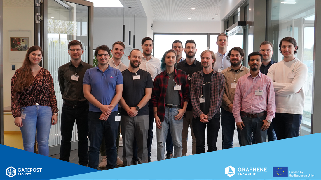
Project team with 8 European partners from science and industry celebrates milestone: Presentation of the first photonically integrated GATEPOST chip.
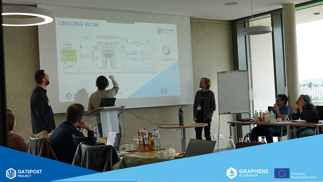
Theodoros Moschos and Chris Vagionas from WinPhoS Research Group (left and centre) and Thomas Van Vaerenbergh from Hewlett Packard Enterprise (right) discuss the first results of the GATEPOST project.
Author bio

Graphene Flagship
Bringing together 126 academic and industrial partners in 13 research and innovation projects and 1 coordination and support project, the Graphene Flagship initiative will continue to advance Europe’s strategic autonomy in technologies that rely on graphene and other 2D materials. The initiative, which builds on the previous 10-years of the Graphene Flagship, is funded by the European Commission’s Horizon Europe research and innovation programme.