


Graphene Week 2015 – reviewing the 2d landscape
Graphene Week 2015 is hosted by the University of Manchester in northern England, and it was from this world-renowned centre of trade, industry and technology that the Nobel Prize-winning revolution in graphene and related two-dimensional materials was launched.
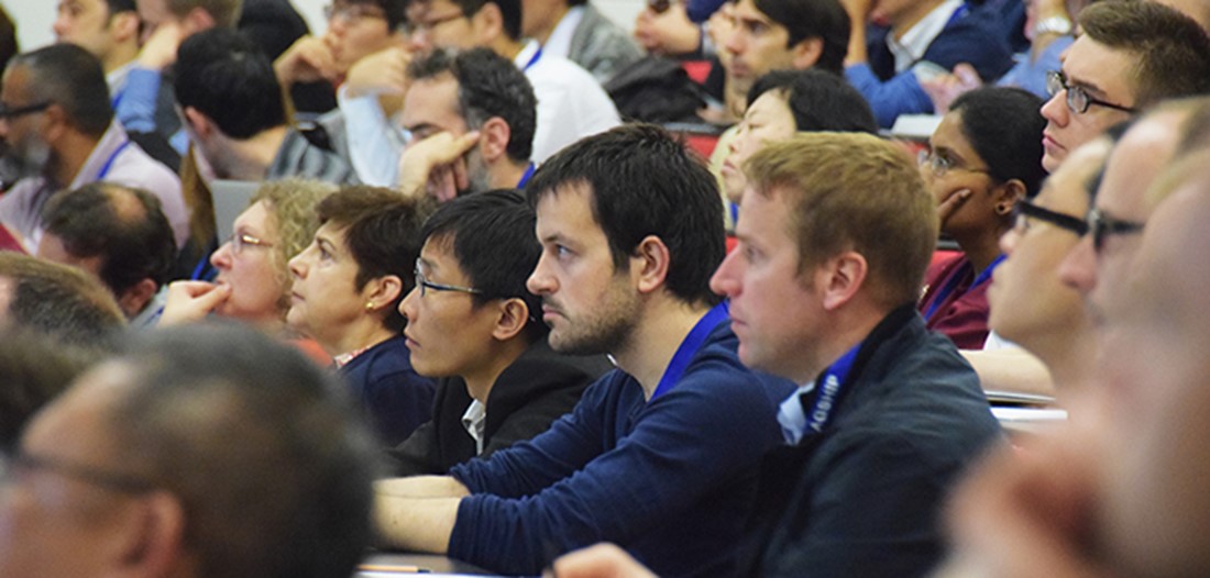
Highlight of the flagship year it may be, but Graphene Week is not about the flagship as a corporate body. It is where Europe’s geographically dispersed and rapidly growing community of two-dimensional materials scientists and engineers come together to discuss their ongoing research and development work, their achievements over the past year, and plans for the period ahead. Morning sessions are taken up with invited presentations, and the afternoons given to contributed talks in thematic sessions, together with fringe meetings and poster presentations.
In a series of articles over the coming days, we shall follow the progress of Graphene Week 2015, with summaries and highlights from the various conference sessions.
Physics near the charge neutrality of graphene
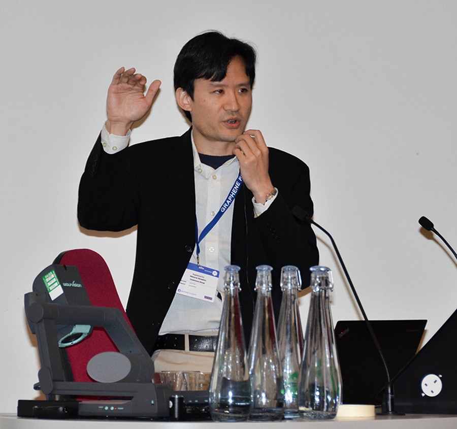
Following the introductory talks, the conference on Monday morning continued with five keynote presentations focused on the bigger scientific picture of graphene and related 2d materials. Harvard University’s Philip Kim began with a reflection on the 10 years since the first Graphene Week.
Kim continued his talk with a look at physics near the charge neutrality of graphene. The Dirac points in graphene – zero energy crossing points of two energy dispersion curves, which define the material as a semi-metal, and therefore devoid of band gap – are an important consideration. The physics here can be exotic, given that, near the Dirac point, physical behaviour is governed by disorder.
Connecting graphene to a superconductor and then reducing the Fermi energy in graphene to a level smaller than that of the superconductor gap, we see evidence of specular Andreev reflections, in which superconducting Cooper pairs split into pairs of electrons and holes across the charge neutrality point. In simple physics terms, this is conservation of momentum at work. In a second example, there is a dramatic enhancement of electronic thermal conductivity in boron nitride-encapsulated graphene at the neutral point, as the Fermi energy there becomes smaller than the thermal energy.
Nanoelectronics based on low-dimensional carbon materials
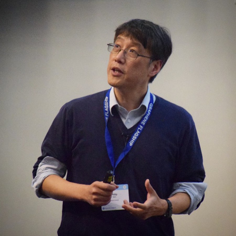
Following Kim, IBM researcher Shu-Jen Han discussed nanoelectronics based on low-dimensional carbon materials. Many of us understand the outline at least of Moore’s Law, which describes the reducing length scale and increasing density over time of microelectronic components. We may also be aware that disruptive technologies are required to extend Moore’s Law to ever smaller physical scales.
Down-scaling transistor size is more than an engineering challenge, as there is fundamental physics to consider. For example, frequency and power limits are saturating at the length scales of tens of nanometres that prevail today. To continue with such scale reduction, power is a critically important factor. But how to reduce power flowing through electronic components?
The problems can be ameliorated by reducing the body thickness of component transistors, and this is where 1d (e.g., carbon nanotubes) and 2d materials (e.g., graphene) can contribute. Han discussed some of the possibilities and challenges involved, and outlined progress made in this area at IBM Research.
Graphene and new carbon materials
After the morning coffee break, delegates heard from Rod Ruoff, a veteran nanoscientist from the US who is now at the Centre of Multidimensional Carbon Materials in South Korea. Ruoff spoke of graphene and new carbon materials, including the material known as bilayer diamond. He also discussed the stacking of graphene layers, the application of ‘negative curvature’ carbon in electrical energy storage, pattern graphite, and graphene coatings that could massively reduce friction.
An important point made by Ruoff is that graphene will not have a major impact until we can produce high-quality bulk material in ways other than chemical vapour deposition. Growth of graphene on copper or other metal substrates is too slow, he said, so we must come up with new methods.
Integrating graphene with silicon
Wolfgang Templ of Alcatel-Lucent in Stuttgart presented his vision for graphene in telecommunications applications. There is much popular talk of graphene and related materials replacing silicon in electronics applications, but according to Templ it is the wafer-scale integration of graphene with silicon components that offers considerable promise at an affordable price.
As a proof-of-concept, Aachen-based research firm AMO has together with Temple and his Alcatel-Lucent colleagues demonstrated a graphene-based photodetector on a silicon waveguide, with transmission rates of up to 50 gigabits per second. Graphene-based optoelectronics is a rapidly developing field, in which basic physics is tightly integrated with the search for practical engineering solutions.
Heterostructures based on 2d atomic crystals
The final presentation on Monday morning was made by Manchester physicist Kostya Novoselov, who spoke of van der Waals heterostructures. These are compound materials built from different 2d materials, the electronic behaviour of which is governed by short-range electrostatic forces.
Novoselov noted that a relatively small number of basic materials define our modern technological world. Electronics is dominated by silicon, civil engineering by steel, and aerospace by aluminium. The trick is in combining materials in ways that provide new potential and capabilities.
In the case of 2d materials, we are rapidly building up a library of such crystals, which may be mixed and matched to engineer new materials – heterostructures – with functionalities tailored for specific practical applications. In his keynote presentation, Novoselov discussed a number of desirable characteristics of such engineered heterostructures, and gave examples of technologies that would benefit from this approach to materials science and engineering.
Setting the scene
Novoselov’s characteristically inspiring talk brought the introductory session of Graphene Week 2015 to a close, and set the scene for the many detailed science and engineering discussions to follow. In follow-up articles we shall look at some of the contributed talks from the parallel sessions.
Photos: copyright © 2015 Anders Frick, Chalmers University of Technology
Harvard University’s Philip Kim began with a reflection on the 10 years since the first Graphene Week.
IBM researcher Shu-Jen Han discussed nanoelectronics based on low-dimensional carbon materials