Enabling Research
Exploring new areas of graphene and related materials research
The Enabling Research Work Package has investigated physical properties of mono- and few-layer graphene, reaching the extreme limits of material purity and electronic transport performance, and exploring the influences of substrates and environments.
The last 10 years
The researchers in this Work Package have developed methods for the transfer of ultraclean graphene in inert atmosphere, followed by encapsulation into hexagon boron nitride (hBN), to create quantum dots and quantum wire circuits based on bilayer graphene with electrostatically controlled spatially modulated band gaps.
The team has worked on Moiré superlattice minibands, which arise when some layered materials are stacked on top of each other with a slight rotation between the layers. We have found a route towards modifying the electronic properties of graphene in highly aligned graphene-hBN heterostructures and twisted few-layer graphene structures.
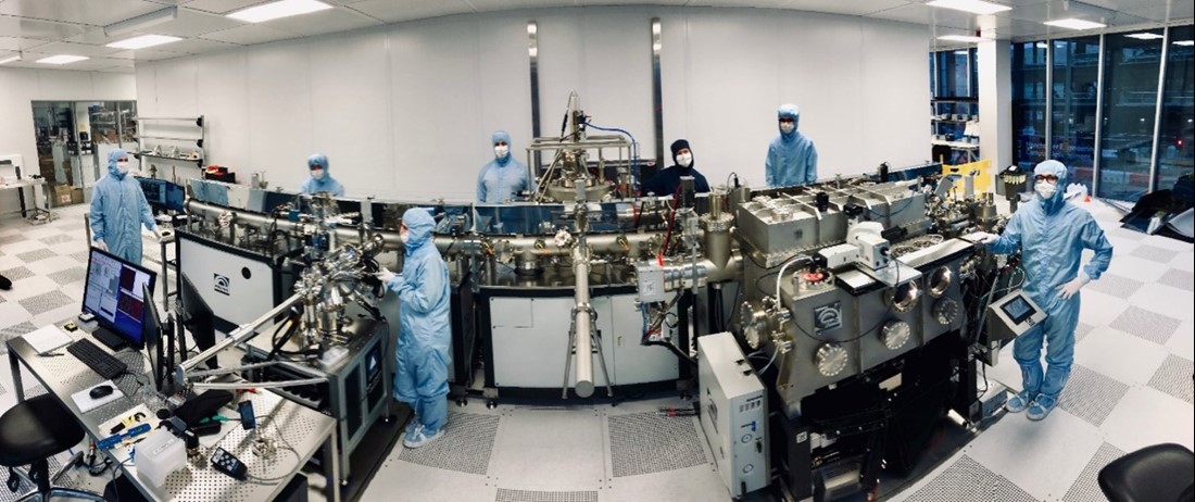
Over the years, the scope of the Enabling Research Work Package broadened onto a wide range of 2D materials: semiconductors (such as transition metal dichalcogenides, indium selenide and gallium selenide) and magnetic layered materials. We developed robotic transfer in glove-box environments and ultra-high vacuums, enabling the fabrication of atomically thin films and heterostructures. Their characterisation and multiscale modelling led to the detailed understanding of their magneto-transport, optical and optoelectronic properties. By controlling the alignment of consecutive layers in the assembled structures, we can implement new materials design, leading to the observation of Moiré superlattice minibands in such structures and the creation of ferroelectric interfaces.
This year’s progress
In 2022 the researchers in the Enabling Research Work Package have created a superconducting quantum interference device (SQUID) using magic-angle twisted bilayer graphene. The researchers were able to control the superconducting charge carriers in the device, measure the inductance and study the current-phase relation of one of the junctions in the device. This can lead to the development of new devices, such as phase-slip junctions and high kinetic inductance detectors.
The researchers also looked closely at the magnetism of chromic sulfide bromide (CrSBr), which could be interesting in the production of new kinds of electronic devices. They found that at low temperatures, the magnetic fluctuations of the material slowed down and the magnetic fields started to change direction in a continuous way. At around 140 K, the magnetic properties change, and the material becomes antiferromagnetic, while at about 40 K, the spin freezes. They believe that the behaviour they observed is caused by a mix of different factors, including the shape of the material and the types of atoms in it.
Finally, the Work Package has demonstrated proof-of-principle field-effect transistors made with mono- or few-layer molybdenum disulphide. The device exhibits a pronounced hysteresis, which means that it could be a promising avenue for the development of new types of electronic and optoelectronic devices with built-in memory functions.


Vladimir Falko, Work Package Leader
Long-term funding, provided by the Graphene Flagship, has enabled us to perform agile open-ended research, addressing new needs and seizing unexpected opportunities, enabling us to achieve fast, valid, high-quality results."
Work Package Leader
References
Portoles, E. et al. Nature Nanotech. 2022, DOI: 10.1038/s41565-022-01222-0
Weston, A. et al. Nature Nanotech. 2022, DOI: 10.1038/s41565-022-01072-w
Lopez-Paz, S. et al. Nature Commun. 2022, DOI: https://doi.org/10.1038/s41467-022-32290-4
Latest Articles

Graphene can do more than transport spins — it can process them
2D Pilot Line launches fourth multi-project wafer run
The 2D Pilot Line (2D-PL), a Graphene Flagship project dedicated to industrialising graphene and other 2D materials for semiconductor applications, announces the launch of its fourth multi-project wafer (MPW) run, marking another milestone in Europe’s growing ecosystem for 2D-material-based device fabrication.

2D Pilot Line Showcases Next-Gen Semiconductor Integration at SEMICON Europa
The 2D Pilot Line (2D-PL) presented its work on integrating two-dimensional materials (2DM) in semiconductor technologies at SEMICON Europa 2025, held at the Munich Messe on 18-21 November 2025. The project — part of the Graphene Flagship — is accelerating the transition of 2DM from lab-scale research toward real industrial integration in photonics and electronics.

2D-PL launches support programme for for MPW runs
Customers of the 2D Pilot Line's (2D-PL) multi-project wafer (MPW) runs can now apply for a 50% reduction in fees in exchange for providing feedback to help the project improve its processes.

Building the Future of Functional 2D Materials with Florian Graßme
Florian Graßme is a researcher working at the intersection of 2D materials and nanosheet functionalisation. Their work in the 2D PRINTABLE project is laying the groundwork for future applications in printable electronics and nano-engineered devices.

Stretching the Limits of Graphene with Robin Smeyers
For Robin Smeyers, a passion for 2D materials began with a single thesis and quickly grew into a full-blown research journey. What started as a master’s project on graphene became a launchpad for academic discovery, leading him to a PhD focused on one of the most intriguing frontiers in condensed matter physics: straintronics. Robin’s work ranges from simulating balloon-like graphene structures to exploring the possibilities of room-temperature superconductors, laying the foundation for technologies that could one day transform our world.

