Flexible Electronics
Developing graphene-based wearable electronics
The Flexible Electronics Work Package takes advantage of the unique properties of layered materials for conductive fabrics as well as elastic and stretchable electronic devices.
The last 10 years
From the beginning of the Graphene Flagship, the target application for graphene-based flexible electronics has been wearable electronics – a megatrend in today’s world. Initially, we focused on bendable and light-weight devices, but our recent efforts have been directed towards elastic electronics for conformable devices, such as skin patches. We have also successfully tackled the modification of textile fibres with graphene for e-textiles.
Our aim has been to investigate the use of graphene in applications where substantial amounts of conductive materials are required, such as printed conductors and heat dissipating materials. Given the increasing number of connected items, the Work Package has continuously tackled high-performance, flexible devices and semiconductors based on transition-metal dichalcogenides (TMDCs), providing the advantage of high-performance devices in flexible structures.
The Work Package has had a strong industrial component. We are actively working to patent graphene-based materials and components for flexible electronics. GRM-elastomers by Printed Electronics Ltd are currently integrated in different demonstrators in collaboration with Interactive Wear AG to enable commercial exploitation. Furthermore, Novalia has designed demonstrators based on graphene and related materials (GRMs) and paper-based substrates, which can be exploited in devices like sensors, biodegradable electrodes and anticounterfeit features.
This year’s progress
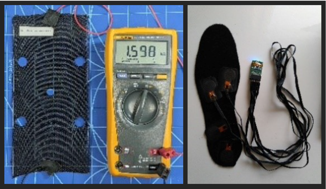
Our team developed a GRM-based conductive polyester (PET) yarn with exceptional performance and durability. We have seamlessly integrated GRMs production with compounding, spinning and weaving processes to create this advanced material. Our ongoing focus is to utilise this material in the development of wearable pressure sensors. As a society, we face an increase in e-waste and the overuse of rare materials. The Flexible Electronics Work Package has increased its efforts towards the use of sustainable technologies through a careful selection of materials, as well as the use of low-energy processing methods, such as printing-based additive methods.
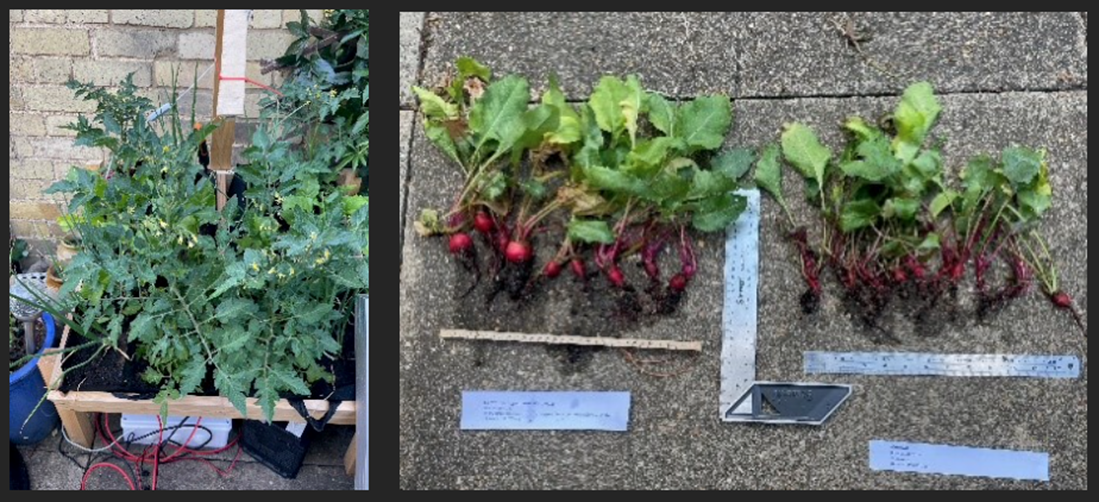
Furthermore, we have successfully developed GRM-elastomers that are washable, and printed stretchable conductors that remain stable even after 1,000 strain cycles. We have also explored various ground-breaking concepts, including paper-based loudspeakers and plant electrodes, which have been developed and tested with positive results. For example, the team is testing GRM- and paper-based biodegradable electrodes that are buried in the soil and powered by solar panels to promote the growth of tomatoes, onions and beetroot: electrically stressed plants appear to grow slightly faster and taller, flowering and fruiting sooner than the control.

Maria Smolander, Work Package Leader
We started with ideas that transformed into concepts close to commercial exploitation.”
Work Package Leader

GRM electrodes in the soil make plants grow slightly faster and taller. Credit: Novalia

Resistance measurement in e-fabric woven with yarn produced by Trevira, another company involved in this Work Package. GRM-PET fabric applied to a pressure sensor in shoe soles. Credit: Interactive Wear
References
van Hazendonk, L.S. et al. Chem. Mater. 2022, DOI: 10.1021/acs.chemmater.2c02007
Munuera, J. et al. 2D Mater. 2022, DOI: 10.1088/2053-1583/ac3f23
Kim, M. et al. Nat Electron. 2022, DOI: 10.1038/s41928-022-00766-2
Pimpolari, L. et al. J-FLEX 2022, DOI: 10.1109/JFLEX.2022.3215928

Tickets with GRM for anticounterfeit technology. Credit: Novalia
Latest Articles
2D Pilot Line launches fourth multi-project wafer run

2D Pilot Line Showcases Next-Gen Semiconductor Integration at SEMICON Europa
The 2D Pilot Line (2D-PL) presented its work on integrating two-dimensional materials (2DM) in semiconductor technologies at SEMICON Europa 2025, held at the Munich Messe on 18-21 November 2025. The project — part of the Graphene Flagship — is accelerating the transition of 2DM from lab-scale research toward real industrial integration in photonics and electronics.

2D-PL launches support programme for for MPW runs
Customers of the 2D Pilot Line's (2D-PL) multi-project wafer (MPW) runs can now apply for a 50% reduction in fees in exchange for providing feedback to help the project improve its processes.

Building the Future of Functional 2D Materials with Florian Graßme
Florian Graßme is a researcher working at the intersection of 2D materials and nanosheet functionalisation. Their work in the 2D PRINTABLE project is laying the groundwork for future applications in printable electronics and nano-engineered devices.

Stretching the Limits of Graphene with Robin Smeyers
For Robin Smeyers, a passion for 2D materials began with a single thesis and quickly grew into a full-blown research journey. What started as a master’s project on graphene became a launchpad for academic discovery, leading him to a PhD focused on one of the most intriguing frontiers in condensed matter physics: straintronics. Robin’s work ranges from simulating balloon-like graphene structures to exploring the possibilities of room-temperature superconductors, laying the foundation for technologies that could one day transform our world.

2D-PL funded to further mature 2D material wafer-scale integration
Launched in October 2024, the Graphene Flagship’s 2D-Pilot Line (2D-PL) project aims to further strengthen the European ecosystem in the development of integration modules for photonics and electronics prototyping services.

