


At the forefront of the rapidly growing market of compound semiconductors
Aixtron’s strengths in metalorganic chemical vapour deposition
Headquartered in Germany, Aixtron has 35 years of experience in deposition systems. It is present in seven countries with a total of about 700 employees. Active in several Graphene Flagship Work Packages, a Spearhead Project and the 2D-EPL, Aixtron works on both growth and transfer tool prototypes. More recently this company provided a 300mm metalorganic chemical vapour deposition (MOCVD) reactor and additional transfer tool prototypes to the 2D-EPL project.
We interview John Walker, development engineer and project leader at Aixtron Ltd in Cambridge, UK, to learn about their recent projects.
Which problems are you trying to solve in your field? Which solutions are you bringing?
I think that the biggest challenge facing graphene adoption is the transition from academia to industrial processes. A lot of proof of concept has been done on graphene and its applications, but the real challenge is how to scale up to the volume and consistency needed for mass production. Since Aixtron has a strong background in bringing research processes to large scale production, we are well placed to add insight and expertise to the community.
Which are Aixtron’s strengths?
We are global leaders in MOCVD technologies. Our MOCVD reactor is the first and most cost-effective choice in the rapidly growing market of 2D compound semiconductors. For instance, LEDs and laser diodes incorporate multiple quantum wells that are typically only several atomic layers thick, while high electron mobility transistors use a 2D electron gas (2DEG) to enable operation at high switching frequencies. Using MOCVD processes, these complex heterostructures can be grown at the scale and uniformity needed for modern industry demands.
Within the Graphene Flagship, who do you collaborate with?
Aixtron is involved with several Graphene Flagship projects. Within Graphene Flagship Work Package for Wafer-Scale Integration and Spearhead Project AUTOVISION, we are developing several graphene transfer technologies and collaborating with Graphene Flagship Partners IIT, imec, ICFO and Qurv Technologies to help automate their processes. For example, we have grown graphene on wafers up to 300mm on our R&D MOCVD systems.
We have also collaborated with the Graphene Flagship's Production Work Package: we have automated roll-to-roll graphene growth technologies for the supply of graphene on foil and wire.
More recently, you have also been involved with the 2D-EPL, what’s your goal?
Both Aixtron Ltd and Aixtron SE are involved in the 2D-EPL’s Wafer Scale Growth and Wafer Scale Transfer Work Packages with imec. We aim to improve and scale up the production of graphene and other layered materials. This includes the growth and subsequent transfer of these materials to target wafers. Our goal is to provide the tools to produce high-quality graphene at 300mm wafer scale and develop new strategies to enable its integration into existing fab production line processes.
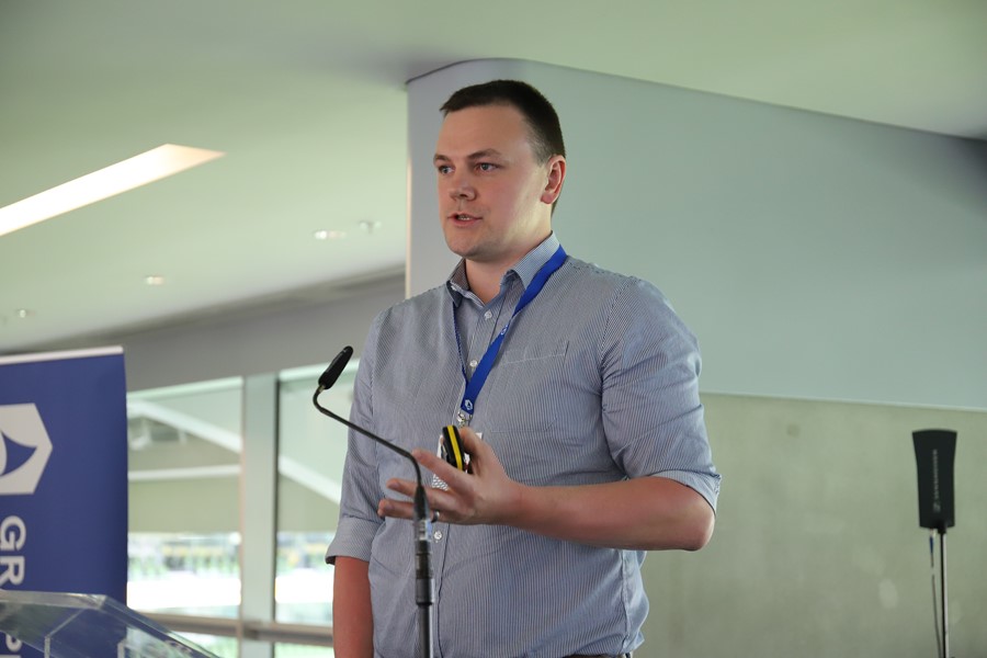
John Walker, development engineer and project leader at Aixtron Ltd
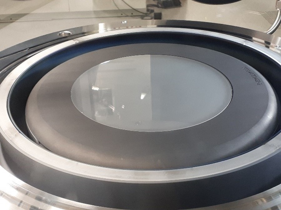
200mm graphene grown on sapphire (Credit: Aixtron)
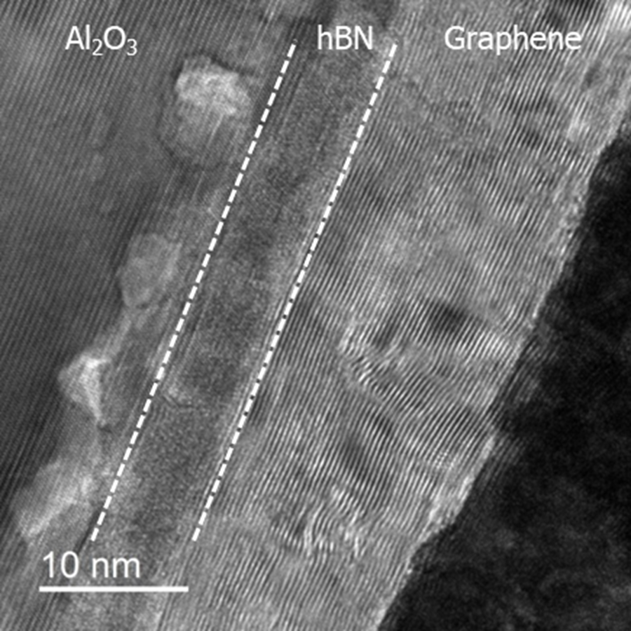
Example of stacked growth of 2D materials by MOCVD (Credit: Aixtron)
Author bio

Letizia Diamante
Science Writer and Coordinator of the 'Diversity in Graphene' initiative.