From lab to fab
Introducing the Graphene Flagship’s new manufacturing facility for graphene-based electronics, optoelectronics and sensors
In October 2020, the Graphene Flagship marked a major milestone toward its commercialisation goals with the launch of the 2D Experimental Pilot Line to integrate graphene and related layered materials into semiconductor platforms. With this new project, the European Commission will invest €20 million in the next generation of electronics and semiconductors.
Graphene and layered materials are ready to hit the market, maturing out of the lab for electronics and optoelectronics applications. The 2D Experimental Pilot Line (2D-EPL) will be the first graphene foundry to integrate graphene and layered materials into semiconductor platforms, keeping Europe at the forefront of this technological revolution. Scaling-up manufacturing is a critical step forward for the advancement of electronic components.
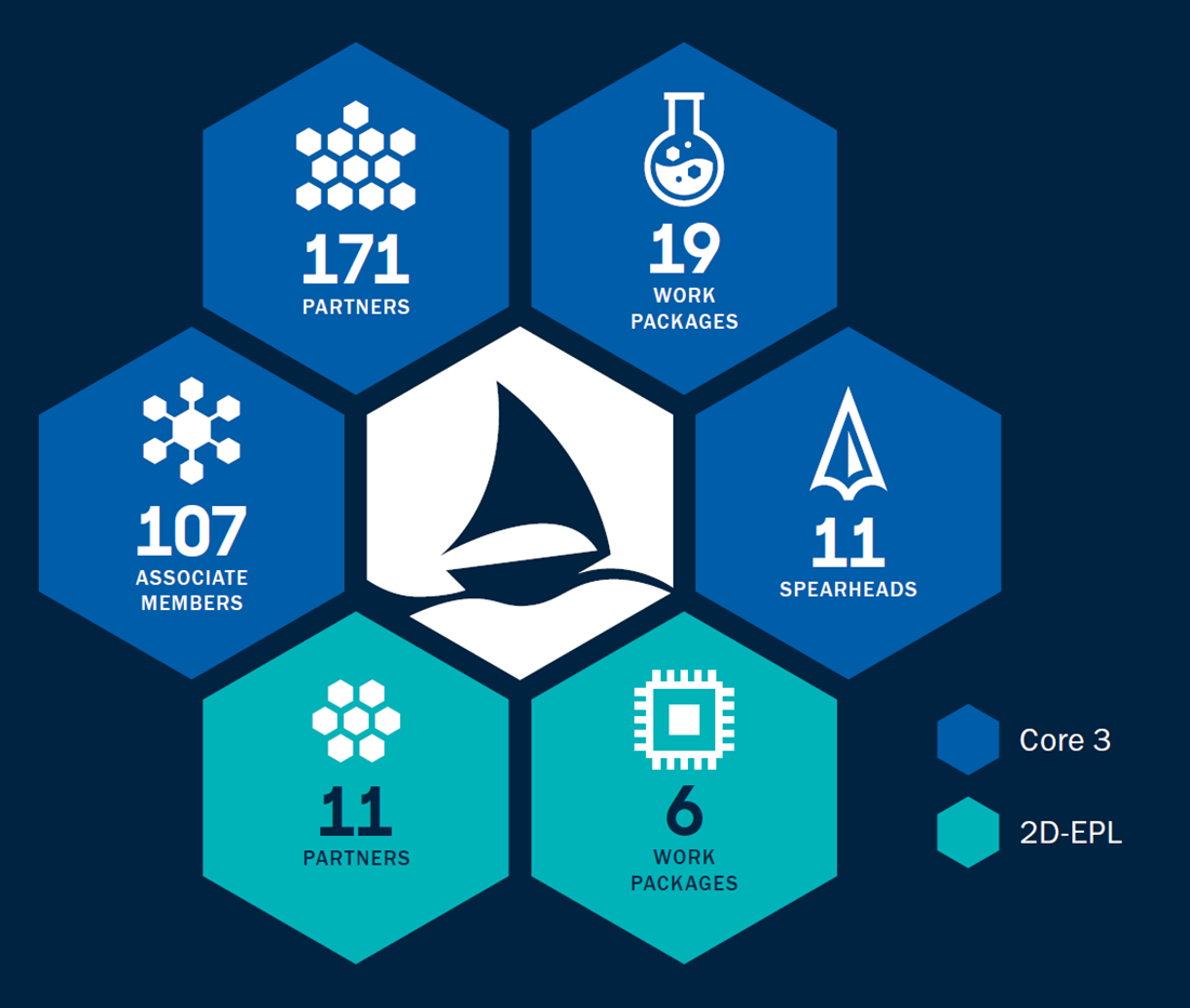
The Graphene Flagship, a ten-year, €1 billion research initiative by the European Commission, has transitioned into Core 3 and the 2D-Experimental Pilot Line – comprising the fourth funding cycle of the project. In this phase, our target is to advance the commercialisation of graphene and layered materials. The Experimental Pilot Line is a major step towards this goal.
Industry in our sights
The goal of the 2D-EPL is to advance the production of electronic, optoelectronic and photonic devices and electronic sensors based on graphene and layered materials beyond the laboratory scale towards industrialisation. As such, it builds an important bridge to facilitate the industrialisation of many of the technologies developed in the Graphene Flagship’s Work Packages and Spearhead Projects, as well as by other European and global customers pursuing the commercialisation of graphene and layered material-based electronic technologies.
During the EC-supported period, the 2D-EPL will develop the processes and practices needed to produce electronic and optoelectronic/photonic applications based on graphene and layered materials, and after the end of the publicly funded period, these services will continue to be provided on commercial terms.

Cedric Huyghebaert, technical leader for the EU-funded 2D-EPL project
Encompassing the entire value chain
Born within the innovative ecosystem pioneered by the Graphene Flagship, the new 2D-EPL will cover the entire value chain, from tool producers and chemical and material providers to manufacturing lines. This collaborative project will integrate several Graphene Flagship members to pioneer the fabrication of new prototype electronics, photonic devices and sensors integrating graphene and layered materials. The 2D-EPL will offer comprehensive prototyping services to companies, research centres and academics, so they can develop and test their innovative technologies based on layered materials.
“By developing a European pilot line for the processing of graphene and layered materials, we aim to bring these innovative materials from the academic laboratories to the semiconductor production lines, making them compatible with the standards in the industry. Moreover, we want to offer early access to experimental pilot line production to the innovative graphene community in Europe. The pilot line will allow them
to scale up the production of their innovative devices based on graphene and layered materials,” explains Cedric Huyghebaert, technical leader for the EU-funded 2D-EPL project, and programme manager for exploratory material and module integration at imec, Belgium.
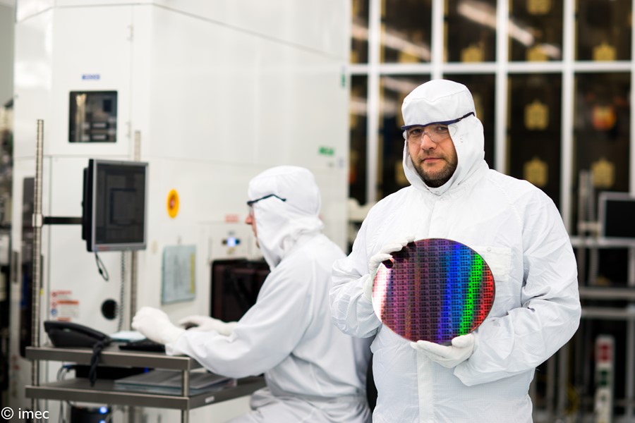
Wafer production is already ongoing in 2D-EPL partner imec’s cleanroom. Credit: imec
New horizons
Combining graphene and layered materials with silicon could enhance the potential of electronic technologies traditionally based on silicon. Nevertheless, integrating both materials on a large scale has been challenging, and until now, advances have progressed at a slow pace – mostly due to a lack of infrastructure. The 2D-EPL will address this challenge, allowing manufacturers to control the interfaces between silicon semiconductors and 2D materials on a large scale.
Collaboration between the 2D-EPL and the Graphene Flagship Core projects will be paramount, as a large number of the potential applications supported by the pilot line are under development in the Graphene Flagship core project. Nevertheless, the focus and organisation of the new 2D-EPL project is radically different. Its objective is to build a long-term plan to overcome the ‘window challenge’ of publicly funded projects, and it will become a sustainable on-demand service for research and innovation in Europe and beyond.
The 2D-EPL will count on expertise from imec, Belgium, which will lead the scientific and technological aspects of the project. The Graphene Flagship team at Chalmers University of Technology, Sweden, will also join the project – providing all of its expertise in management and communication. Moreover, the pilot line will be supported by a core technical steering group consisting of principle investigators from different partners of the project, and it will be overviewed by an Industrial Advisory Board, integrated with key players from the European semiconductor industry.
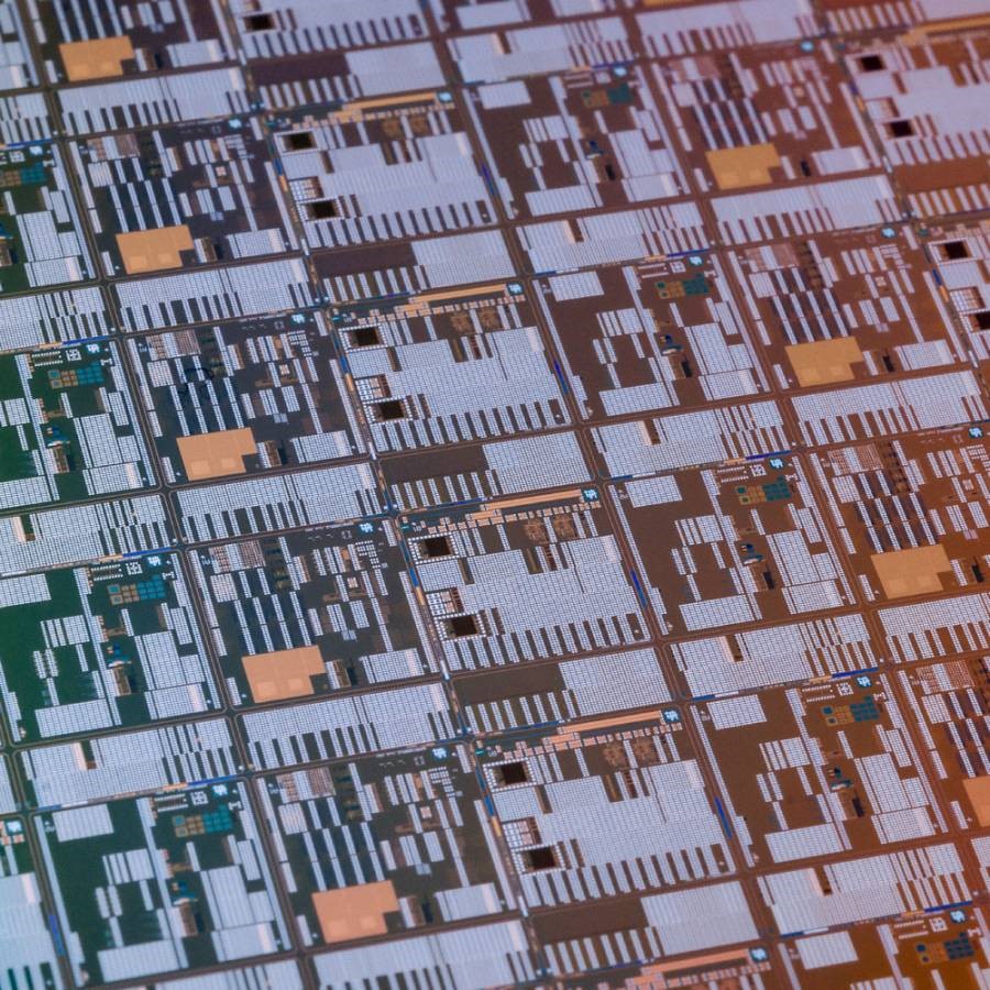
Integrating graphene and layered materials in silicon wafers could revolutionise the electronics industry. Credit: imec
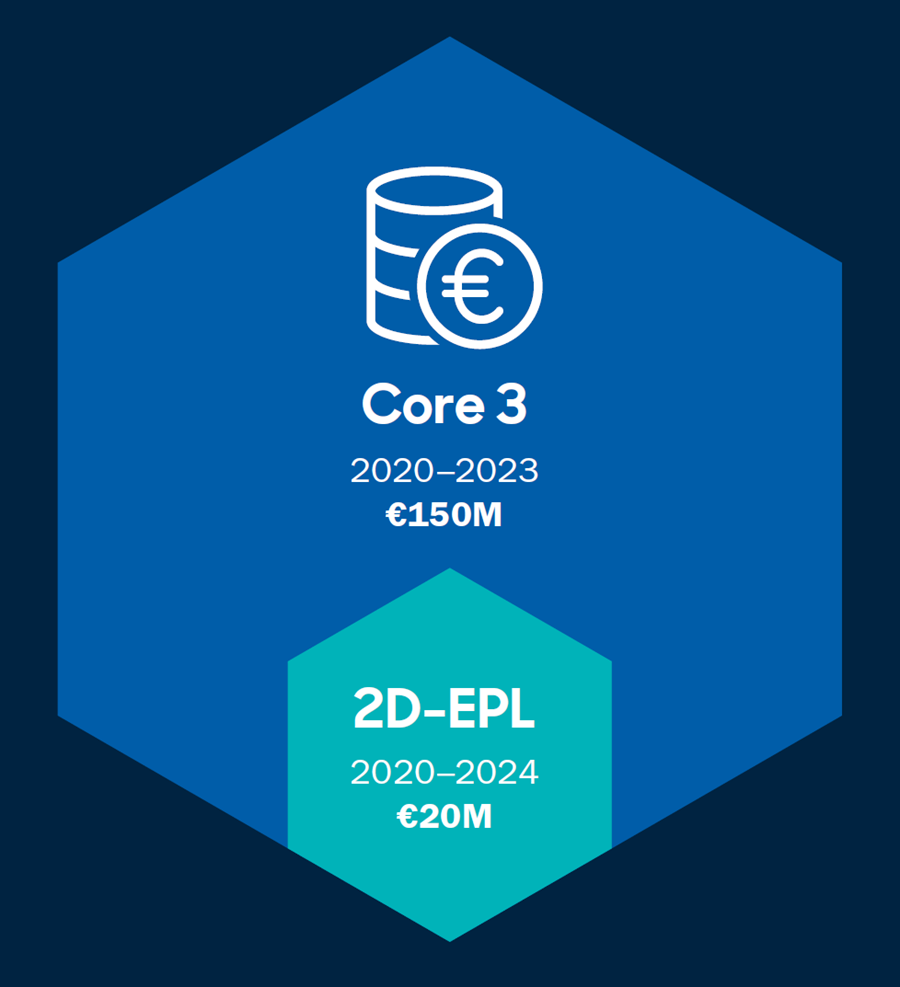
With the launch of the 2D-EPL, the Graphene Flagship now administers two separate European Commission projects that will run concurrently and collaboratively.


