


High Performance Graphene Photodetectors Set Speed Record
Fast Photodetector Device.
Graphene is an ideal material for optical communications systems. A new, waveguide-integrated photodetector design sets a record high bandwidth for ultrafast, high data rate graphene devices.
Graphene-based technologies are proving integral to the new generation of communications – enabling high performance optical communication systems through ultra-fast and compact optoelectronic devices. Researchers from the Graphene Flagship working at TU Vienna, Austria and AMO, Germany, have demonstrated ultrafast photodetectors that have the highest reported bandwidth for graphene-based devices, enabling data rates of up to 100 Gbit/s. The research, recently published in Nano Letters, points the way towards graphene applications in high-speed communications systems.
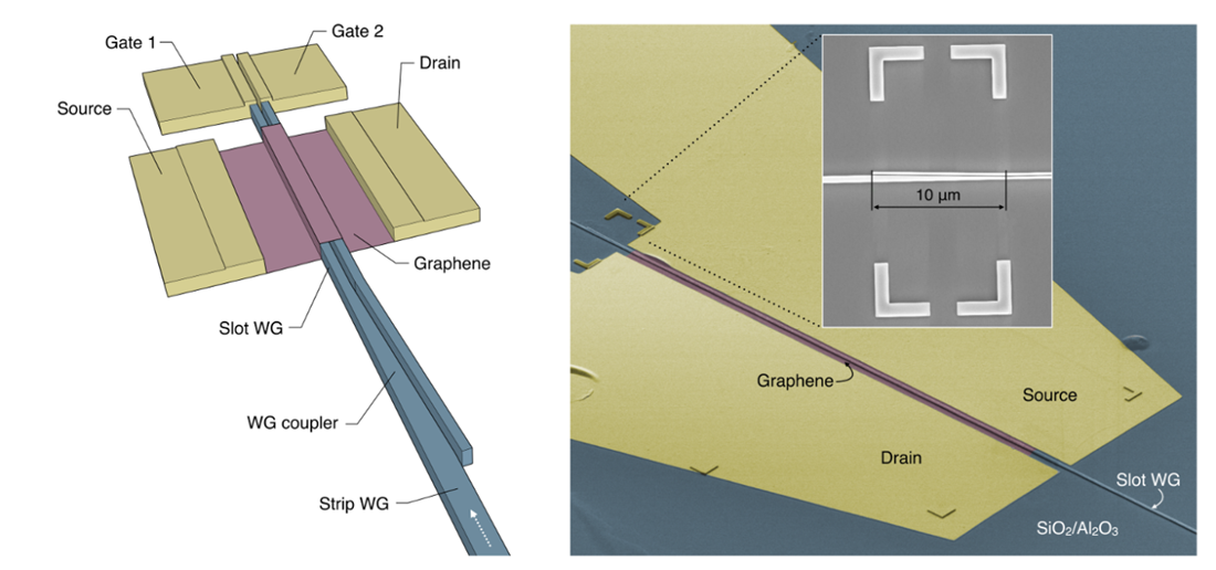
Image reproduced with permission from [1]. Copyright: 2016, American Chemical Society
Next-Generation Communications
Modern telecommunications systems are built on the conversion of light into electrical signals, for example in optical links in fibre-optic communications systems. Photodetectors within these systems convert light into voltage signals, which are then processed for use in computers, phones, and other devices. Current optical detection systems are based on silicon and other semiconductors such as germanium, and are reaching their limits in terms of speed and bandwidth.
Simone Schuler, a researcher at TU Vienna, explained the importance of increasing data capabilities. “These kinds of photodetectors are typically used in optical data links, which form the back-bone of the internet. The maximum operation speed of a photodetector defines the maximum data rate the detector can receive. So, the faster the photodetector the more data it can receive.”
As more and more devices are connected to each other, the demands on large-scale communications systems grow rapidly. Next generation communications systems must be able to handle the large number of connected devices in the Internet of Things (IoT), so faster optical detection and higher bandwidths are needed to keep data transfer reliable between all connections. As well as the internet and next generation mobile communications, such as 5G, such photodetectors also have applications in radar for industrial automation, known as Industry 4.0.
Ultrafast Photodetectors
Graphene’s properties make it ideal for next-generation optoelectronics and optical communications systems. Its excellent electrical properties and broadband optical absorption are highly suited for high-performance optoelectronic devices, and it can be readily integrated with silicon photonic systems. The photodetector demonstrated here is highly sensitive, due to its very compact structure. This enables the use of such detectors alongside other opto-electronic devices including switches in functionally dense, integrated chips. “This could open the path towards a complete integration on one CMOS chip. Graphene will be the enabling material for realising high performance photodetectors on a silicon platform,” added Schuler.
In the new photodetectors, light is guided into a slot waveguide that is covered with graphene. Under specific electrical conditions in the graphene, in which the graphene acts as semiconductor junction, the light in the waveguide generates a current in the graphene via the photothermoelectric effect, converting light into an electrical signal. The sensitivity of the detector can be tuned electrically without compromising the speed, enabling the high bandwidth and ultrafast data rate.
Speaking about this new photodetector design, another of the paper’s authors, Daniel Neumaier of AMO, Germany said “This is an important step towards high performance on-chip photo-detectors, demonstrating that competitive speed and sensitivity can be achieved in graphene photodetectors in a highly controlled way.” On-chip integration of different graphene-enable technologies is an important focus of the Graphene Flagship. Neumaier leads the Graphene Flagship Electronics and Photonics Integration Division and Work Package Electronic Devices, and is a member of the Flagship Management Panel and Executive Board.
On-Chip Integration
In order to take new technology such as this to direct, real-world applications in communications networks, it must be possible to put the technology onto optoelectronic chips. “The next step towards applications will be the transition into a CMOS line, which is one focused activity in the Electronics and Photonics Integration Division of the Graphene Flagship project,” said Neumaier. CMOS manufacture has strict requirements for materials and processing, so translating laboratory techniques into methods suitable for chip production is very tricky.
Marco Romagnoli, of the National Consortium for Telecommunications (CNIT), Italy, is the leader of the Graphene Flagship Wafer-Scale Systems Integration Work Package, and spearheading the development of silicon-compatible processes for mass production of graphene-based electronics. “We are developing the key building blocks to be integrated in graphene photonic circuits. This detector is a good example of design compliant with the platform under development in the Flagship, and the combination of good performance with technological compatibility is key to move forward in the progress of graphene technology for electronics and photonics applications,” he said.
This research is a prime example of the way graphene can provide improvements over existing optoelectronic technologies, both in terms of performance and compactness. Frank Koppens, of the Institute of Photonic Sciences, Spain, is leader of the Flagship’s Optoelectronics and Photonics Work Package. “This work has shown record-high performance and operation with zero dark current. It’s a major step forward for the Flagship program that aims at developing the components (detectors, modulators) for a fully CMOS-integrated optical data-communication platform,” he said.
Andrea Ferrari, Science and Technology Officer of the Graphene Flagship and Chair of its Management Panel, stated "Graphene photonics and optoelectronics is clearly one of the strongest areas for mid-term development. The Graphene Flagship has made significant investment in pioneering large scale integration of optoelectronic components based on graphene and related materials. This is a key step to enable their widespread uptake in the future of data com and IoT areas. This result clearly shows that we are on the right track on our technology roadmap"
The Graphene Flagship is dedicated to exploring the potential for graphene and related materials in new technologies in a wide range of areas, from telecommunications and sensors to building materials and batteries. The specific properties of graphene have a lot to offer in innovative technologies, and taking graphene from the laboratory to commercial application is a cornerstone of the Graphene Flagship.
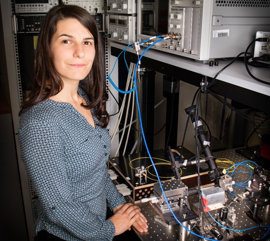
Simone Schuler, TU Vienna
Graphene will be the enabling material for realising high performance photodetectors on a silicon platform”
TU Vienna