


Layered materials grant sight to electronic chips
Chip based on layered materials serves as both an image sensor and a neural network, classifying images a thousand times faster than conventional machine-vision systems
Researchers at Graphene Flagship Partner Vienna University of Technology in Austria reported in Nature an image sensor based on layered materials, with an integrated artificial neural network (ANN) capable of learning, and then classifying simple images within nanoseconds. The chip is a thousand times faster and uses much less power than conventional vision technologies.
In this article, read on to learn about image sensors and neural networks – and explore the possibilities of this unprecedented device.
A multitasking image sensor
When you take a photo, your smartphone is generally able to identify faces in the scene and mark them with a circle or rectangle. This is possible because an image sensor captures the visual information and passes it on to the processing units, which convert the optical signals into digital output. This movement of data between the sensor and processing units is relatively slow, on the order of microseconds, and requires a relatively high power consumption. If you are taking a selfie, this delay is not a big problem, but it can have major drawbacks for high-tech scientific applications.
In this study, the Graphene Flagship researchers devised an image sensor that can simultaneously capture and process images, making object recognition many orders of magnitude faster. Furthermore, this device does not consume any electrical power when it is operating, since the photons themselves provide the energy for the electric current.
Artificial neural network for brain-inspired artificial learning
The sensor is complemented by an ANN, a man-made system inspired by our brain. In the brain, neurons can influence the activity of their neighboring neurons, as they are connected to each other via synapses. In ANN, components dubbed "neurons" are fed data and cooperate to tackle a problem: in this case, recognising an image. The neural network repeatedly adjusts the strength of the connections, or ‘synapses’, between its components. Attempt after attempt, the network discovers the best solution and adopts it to solve the problem quickly.
Image sensor + artificial neural network = machine vision technology
The researchers in Vienna devised sensors containing nine pixels – the ‘neurons’ – placed in a 3x3 array. Every pixel in turn, consists of three photodiodes, which are semiconductor devices that convert light into electrical current, that provide three outputs. Each photodiode links its pixel to the other 8 pixels.
The photodiodes are made of sheets of tungsten diselenide, a layered semiconductor with a tunable response to light. Each photodiode is tuned to increase or decrease its sensitivity to light using an applied voltage. In comparison, photodiodes based on silicon would exhibit a fixed responsivity and would not be suitable for the proposed application.
The current from each photodiode is determined by the intensity of incoming light and the voltage across it. Each neuron sums the individual currents coming from the other 8 neurons, and the combined values are then fed into a computer.
How to train your chip
The researchers used the chip to classify three letters of the alphabet (n, v or z) shone on the chip with a laser beam.
A computer is initially connected to the device. The training starts by assigning random photoresponse values to all photodetectors. Starting from this, it is possible to calculate how to change the photoresponsivity values to bring the output (the letter that the device “sees”) closer to the desired one (the letter that is effectively shown to the device). The researchers tweak the photoresponsivity of each photodiode by tuning the split gate voltage of each photodiode.
By repeatedly showing a set of noisy letters to the chip and then calculating how to change the photoresponsivity values, the chip learns to correctly identify all the projected letters, even when they are very noisy. After multiple re-adjustments, the device yields the right answer repeatedly. Then, the computer is no longer needed, so the neural network can work alone and generate a reply – a numerical code corresponding to one of the three letters – in just 50 nanoseconds.
The device can classify images after a series of training processes (supervised learning), but it can also recognise a characteristic component or structure of an image from input data, without extra information (unsupervised learning).
Moving from AI to hardware: speed, scale and possible applications
Usually, artificial intelligence is based on software, but this new sensor is a step towards AI chips.
The speed sets this device apart from conventional machine vision. Conventional technology is usually capable of processing up to 100 frames per second, with some faster systems capable of working up to 1,000 frames per second. In comparison, this system works with an equivalent of 20 million frames per second.
Currently, the device deals with simple images, but it could be scaled up with today’s technology and find applications in different fields, such as fluid dynamics, high-energy physics, combustion processes or mechanical breakdown.
Furthermore, at the moment, each photodiode requires two external digital-to-analog converters to apply the split gate voltages. To overcome this limitation, the researchers have shown that the split gate voltage can be stored in the device itself by making use of a floating-gate memory. With this trick, the voltage is created by storing the electric charges in the floating gate for an extended time, up to several years.
“Scaling the devices up, this neuromorphic approach can play out its strengths in the realm of image recognition and processing. We are also considering other ideas, like improving the light absorption or extending the spectral range into the infrared,” explains Lukas Mennel, first author of this study. “In principle, the capabilities of this device are not only limited to visual data. Any kind of data could be (pre)processed with an artificial neural network in the sensor itself. For example, audio or olfactory neuromorphic sensors could be developed for rapid on-chip processing.”
Frank Koppens, Graphene Flagship Work Package Leader for Photonics and Optoelectronics, says: “This impressive work shows a completely new application of layered materia-based cameras, taking advantage of its unique properties like its in-situ tunability. Neural network image sensors will impact society in many different ways, and with layered materials the high-speed requirements have now been met.”
Andrea C. Ferrari, Science and Technology Officer of the Graphene Flagship and Chair of its Management Panel, added: “This work is another major milestone for the Graphene Flagship. The Flagship is clearly world-leading when it comes to the integration into chips of layered materials. These advanced building blocks will underpin the development of new state-of-the-art technologies.”
Reference
Mennel, Lukas, et al. "Ultrafast machine vision with 2D material neural network image sensors." Nature 579.7797 (2020): 62-66.
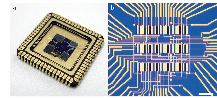
Images of the vision sensor. (a) The chip used in this study mounted on a chip carrier, which has a side length of around 2.5 cm. (b) Microscope image of the photodiode array which consists of 3x3 pixels. Each pixel includes three photodiodes. Scale bar: 15 µm. Credit: Vienna University of Technology
Author bio

Letizia Diamante
Science Writer and Coordinator of the 'Diversity in Graphene' initiative.