


Ultrasharp patterning of layered materials
Patterning small and sharp geometries for the quantum technologies of the future
Researchers at Graphene Flagship Partner Technical University of Denmark (DTU) have taken the art of patterning nanomaterials to the next level with a clever strategy that downsizes nanopatterns below the current limit.
Layered materials, such as graphene, are one of the most significant research topics in physics and materials sciences. One of their key features is perhaps their programmability: by creating customized nanopatterns in these materials, one can tune their optical, electronic, chemical and mechanical properties, and create essential components for electronics, spintronics and valleytronics devices, with better performance and much lower power consumption than today's technologies. These super-small structures can be used in very compact and electrically tunable metalenses – special lenses with intriguing refractive properties (e.g. negative refractive index) – which can be applied to high-speed communication and biotechnology.
DTU scientists have patterned layered materials using electron beam lithography, a system that exploits electrons to print patterns, with a resolution of approximately ten nanometers. However, the most advanced applications require a higher resolution and denser patterns than these lithography systems can provide.
“If we really want to unlock the treasure chest for future quantum electronics, we need to go below ten nanometers and approach the atomic scale. In 2019, we showed that circular holes placed with just 12-nanometer spacing turn graphene into a semiconductor. Now we know how to create circular holes and other shapes, such as triangles, with nanometer sharp corners in graphene and other materials, and this allows us to dial in way more sophisticated electronic behaviours,” explains Peter Bøggild, professor and group leader at Graphene Flagship partner DTU, in Denmark.
DTU researcher Lene Gammelgaard describes their approach. They use a hexagonal boron nitride (hBN) crystal on the top of the material they want to pattern, such as graphene or graphite, creating concentric, “bull’s eye” holes that are larger for hBN and smaller on the underlying material. “Suppose we make a circular hole with a diameter of 20 nanometers on the hBN crystal, then the hole in graphene can be downsized to 10 nanometers, or smaller. If we make a triangular hole on the hBN crystal, the downsizing process cuts a smaller triangle with self-sharpened corners in the graphene layer. Usually, creating smaller patterns tends to lead to more imperfections, but this is not the case with our technique,” says Gammelgaard.
“This is an exciting and useful technique. It will benefit the thousands of researchers around the world who are pushing the limits of layered materials nanoelectronics and nanophotonics,” adds Dorte R. Danielsen from DTU.
“Reducing the feature size of electronic components was the driving force in microelectronics in the past 50 years, enabling the integration of more and more transistors on one chip, known as Moore’s law. This device shrinkage has started to slow down in recent years, as the required lithography technology is facing physical and especially economic boundaries. The DTU team has now presented a novel approach of reaching smaller feature sizes on layered materials than normally possible with common lithography techniques. This approach demonstrates that new and clever solutions offer an opportunity to go to smaller feature sizes using existing lithography tools,” says Daniel Neumaier, Leader of Graphene Flagship Work Package Electronic Devices.
Andrea C. Ferrari, Science and Technology Officer of the Graphene Flagship and Chair of its Management Panel, adds: “Graphene-enabled electronic and spintronic devices have performance already competitive with the state-of-the-art of traditional approaches. This work demonstrates a new patterning technique that will allow future devices to reach unprecedented performance, and showcases another process innovation brought about by the Graphene Flagship.”
References
Jessen, Bjarke S., et al. "Lithographic band structure engineering of graphene." Nature nanotechnology 14.4 (2019): 340-346.
Danielsen, Dorte R., et al. "Super-Resolution Nanolithography of Two-Dimensional Materials by Anisotropic Etching." ACS Applied Materials & Interfaces (2021).
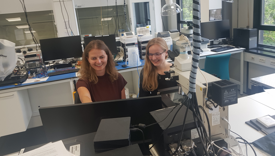
Lene Gammelgaard (left) and Dorte Danielsen (right) working on new nanopatterns. (Photo credit: DTU)
This is an exciting and useful technique. It will benefit the thousands of researchers around the world who are pushing the limits of layered materials nanoelectronics and nanophotonics.
Researcher at Graphene Flagship partner DTU, Denmark
Author bio

Letizia Diamante
Science Writer and Coordinator of the 'Diversity in Graphene' initiative.