Jump to content

2D-EPL multi-project wafer run 4


EU Funded

The 2D-EPL project has launched its fourth multi-project wafer (MPW) run where universities, research institutes and companies can include their designs as dies on joint wafers. This run is mainly intended for graphene sensors, and will be offered by VTT. 

Why apply?

  • Customisable chips
  • Short turn around
  • Flexible process flows
  • Direct communication channels
  • Experienced partners
  • Feasibility consulting
  • CMOS readout integration

Important Dates

  • June 2023: Call open, see specifications below
  • 30 September 2023: Call closes, PDK available
  • 31 January 2024: CMOS design freeze​
  • 30 May 2024: Post-processing design freeze
  • 31 July 2024: CMOS wafers ready
  • 31 October 2024: MPW run delivery target ​

Price

  • 40 k€ including one post-processing design and 40 dies​
  • Additional post-processing designs 2 k€ per design​
  • Additional 20 dies 3 k€​

CMOS design options 

(price negotiated separately)​

  • Customer design​
  • VTT designs ​
  • VTT design services ​

This run is now closed, stay tuned for our next MPW run.

The offered baseline process for the fourth MPW run is a CMOS integrated GFET including via, back gate, bottom contact, graphene and encapsulation modules. The design of the device can be adjusted within the specifications listed below.

Specifications

Application

  • GFETs for Bio/Gas/Chemical sensors, Hall Sensors, Photodetectors
  • CMOS readout integrated sensors
  • Large sensors arrays with multiplexing and integrated readout

Substrate

  • 200 mm Si CMOS wafer​
  • XFAB’s XH018 process​
  • Die size: 5 mm x 5 mm ​

Key parameters

Schematic of the baseline design.

A CMOS integrated GFET sensor array for biosensing (left) and gas sensing (right).

VTT, Micronova in Espoo, Finland

About VTT

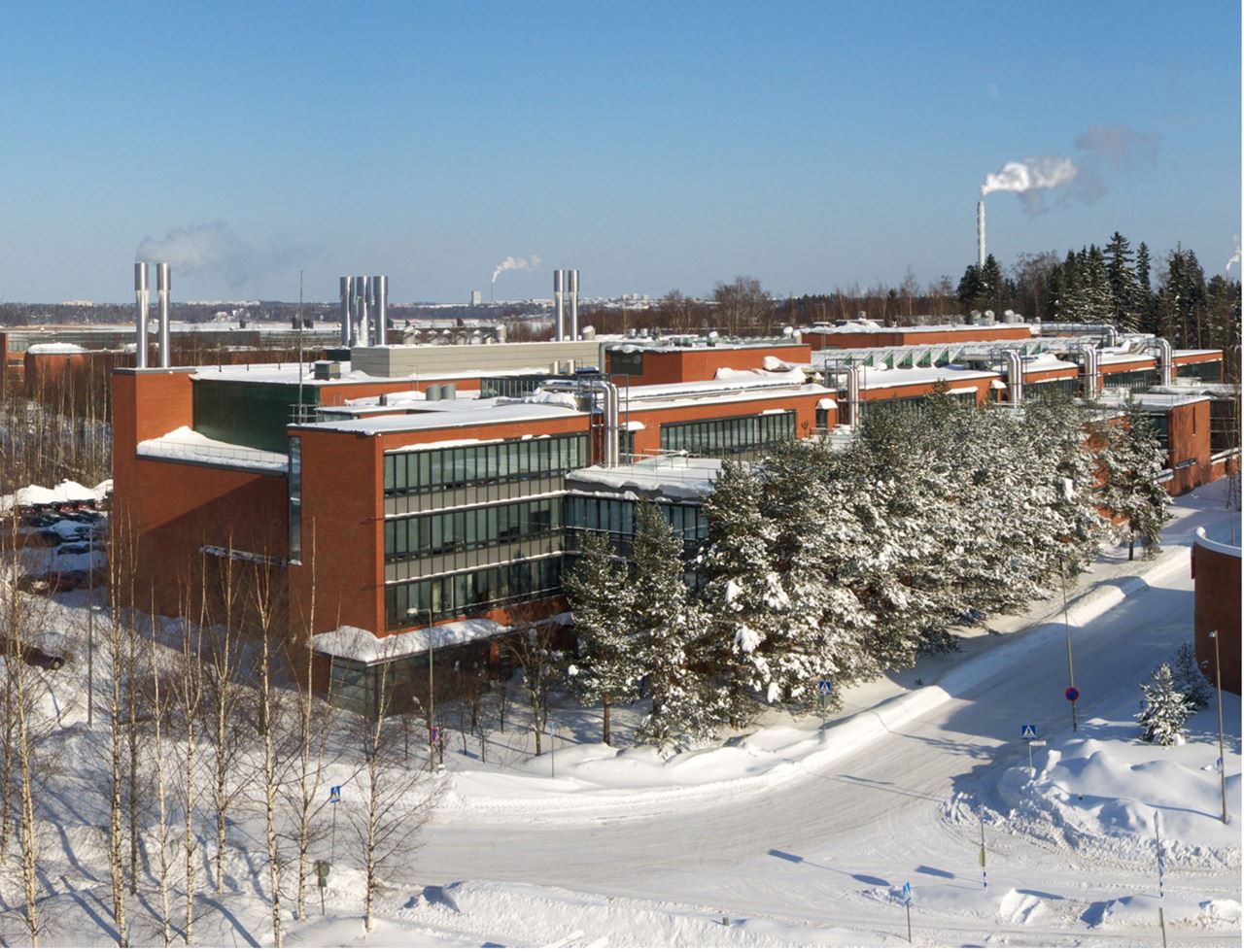
VTT Technical Research Centre of Finland Ltd is a state-owned non-profit research and technology organisation (RTO) with the aim of strengthening Finnish and European industrial competitiveness in multiple fields ranging from sustainable food and energy production to quantum computing. As an RTO VTT acts between universities and industry, bringing basic research towards industrial adaptation and helping the industry in their R&D needs. Graphene industrialisation at VTT is based on 2 600 m2 cleanroom in Micronova, Espoo, with a focus on wafer-scale CVD graphene process optimisation for electronics, photonics and sensors, including the integration on silicon CMOS for multiplexed sensor arrays. In addition to the MPW runs, VTT offers contract research, prototyping and small-scale manufacturing.