


2D-EPL MPW run in production
A step-by-step look at the 2D-EPL’s first multi-project wafer run
The 2D Experimental Pilot Line (2D-EPL) is a Graphene Flagship project created to address the challenges of establishing reliable fabrication processes for high-volume production of graphene and related materials (GRM) based electronics, photonics and sensors. Part of this process is the development of multi-project wafer (MPW) runs in which customer designs are included as dies on joint wafers. This article will take us through the manufacturing steps involved in the 2D-EPL’s first MPW run. Future runs will operate in a similar fashion, though they will be tailored to different applications and build on the experience of past runs.
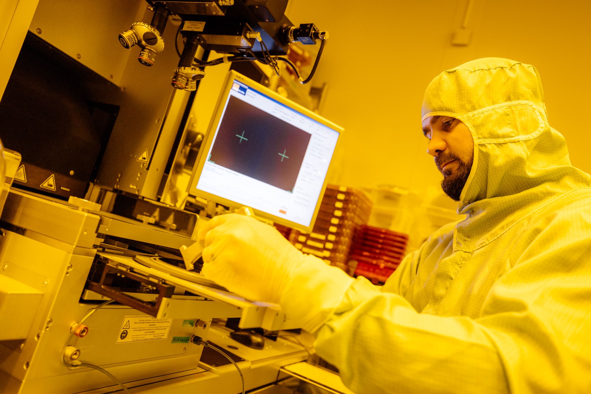
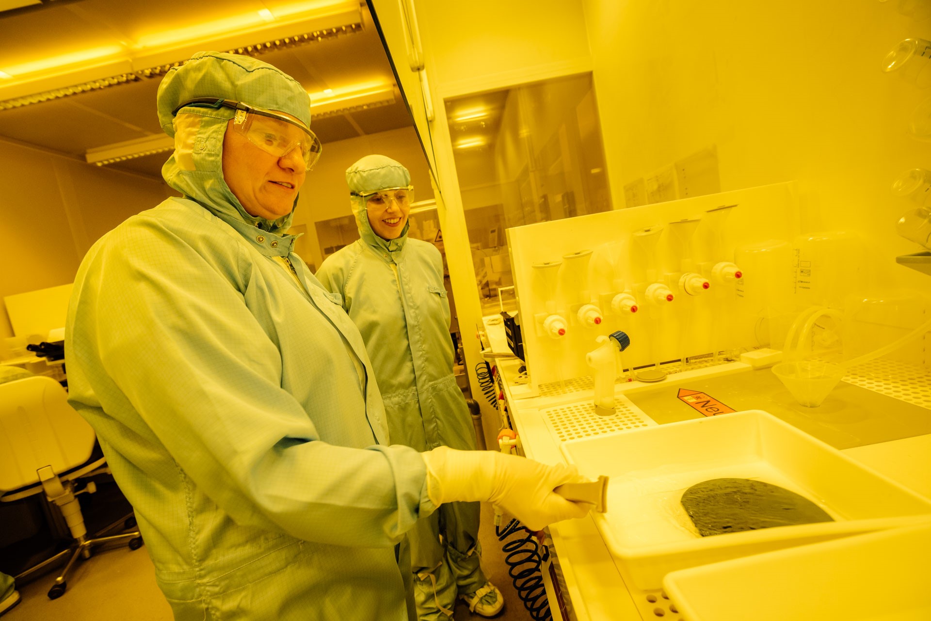
STEP 1: BACK GATE AND CONTACTS
The fabrication process includes several metallisation steps to deposit the back gate as well as the bottom and the top contacts. Each metallisation step is formed by four sub-steps (coating, UV contact lithography, development, metal evaporation, and lift-off).
Step 1


STEP 2: DIELECTRIC DEPOSITION
The gate dielectric (Al2O3-layer) is deposited using atomic layer deposition (ALD).
Step 2
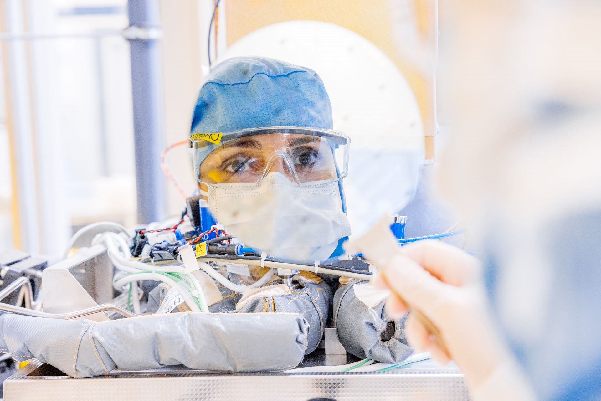


STEP 3: GRAPHENE TRANSFER AND PATTERNING OF GRAPHENE
The graphene is grown by Graphenea (Spain), who then transfer it onto the wafer. After the transfer, the wafers are sent back to AMO where it is patterned in the desired shape using reactive ion etching and plasma etching.
Step 3


STEP 4: CONTACTS AND ENCAPSULATION
After graphene is patterned, the wafers undergo a final metallisation step when the top contacts are fabricated, followed by encapsulation with Al2O3.
Step 4
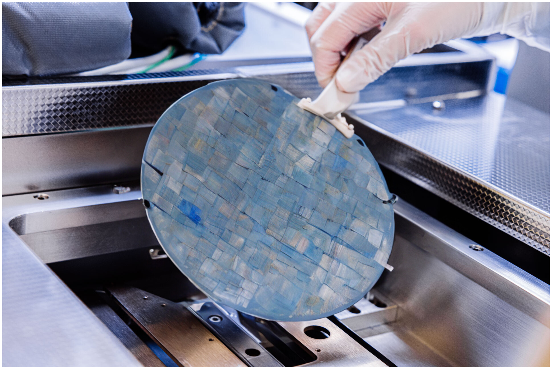
STEP 5: OPENING OF ENCAPSULATION
For encapsulation, the wafer goes through another round of coating, lithography, development, evaporation and lift-off to open the contact pads and the graphene area of the sensors.
Step 5


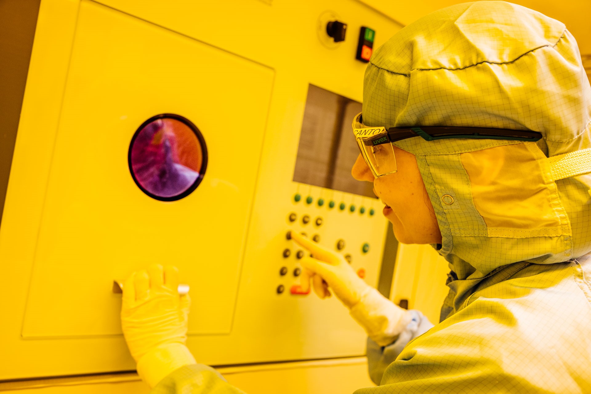
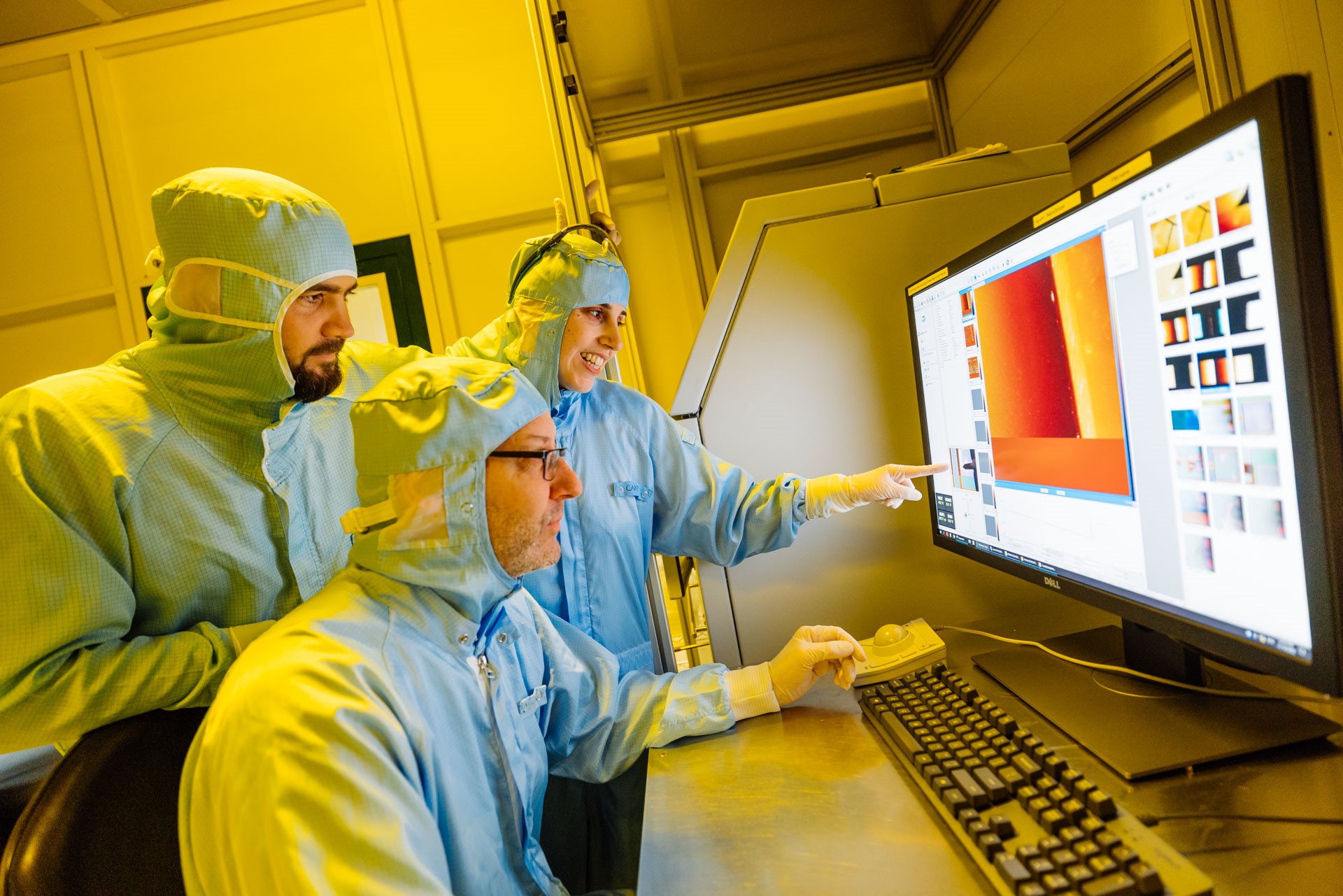
STEP 6: TESTING
Finally, the wafers are extensively tested using optical microscopy, Raman spectroscopy, as well as electrical measurements on test devices.
Step 6


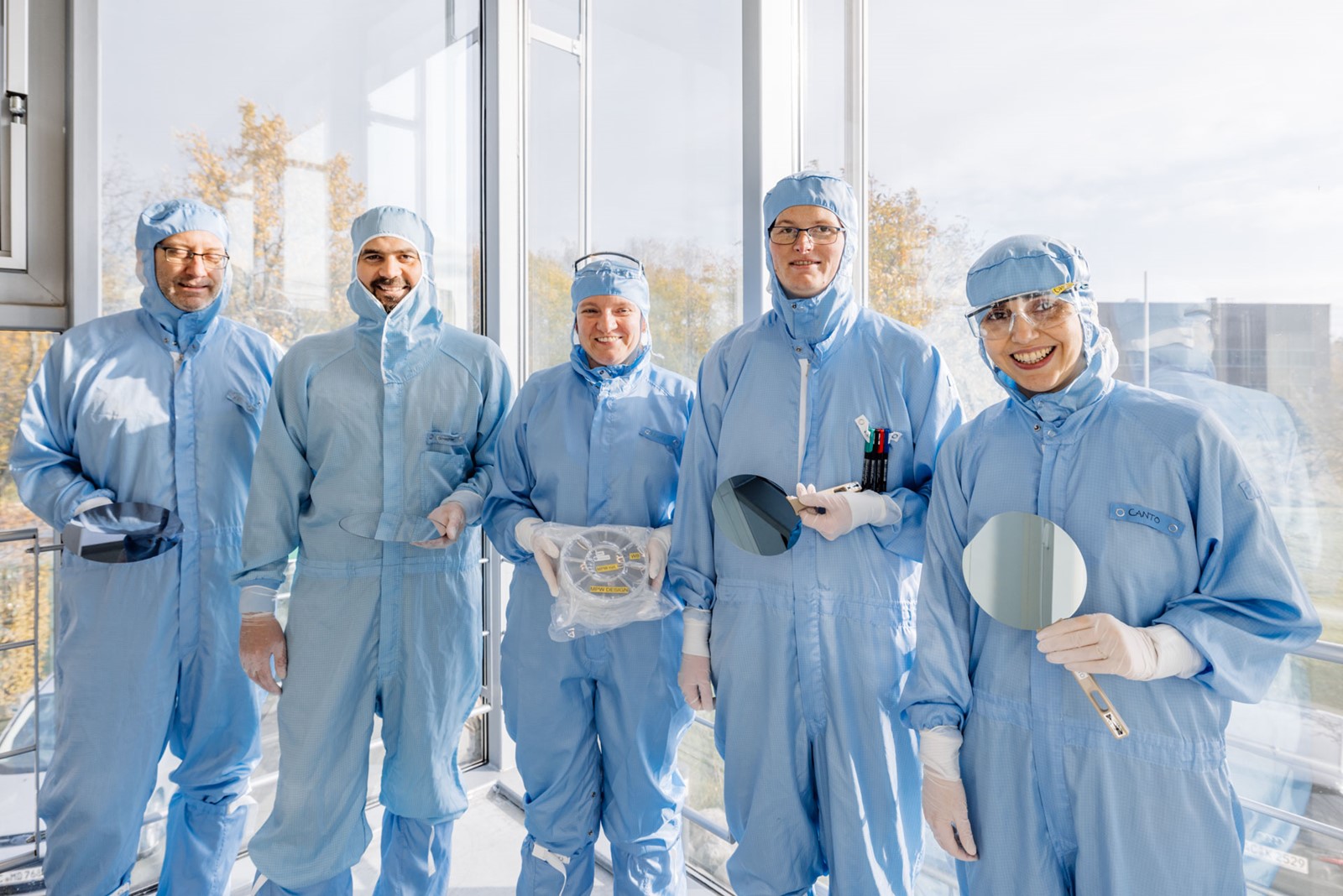
AMO team celebrates a job well done!
Learn more about the 2D-EPL's upcoming MPW runs here.
Author bio

Graphene Flagship
Bringing together 126 academic and industrial partners in 13 research and innovation projects and 1 coordination and support project, the Graphene Flagship initiative will continue to advance Europe’s strategic autonomy in technologies that rely on graphene and other 2D materials. The initiative, which builds on the previous 10-years of the Graphene Flagship, is funded by the European Commission’s Horizon Europe research and innovation programme.