


AIXTRON installs a MOCVD machine CCS 2D in IMEC’s fab
Aiming to reach the best 2D-materials reproducibility for the lab-to-fab
Within the 2D Experimental Pilot Line framework, an 200/300 mm compatible Metal-Organic Chemical Vapour Deposition (MOCVD) reactor, produced by AIXTRON (Germany), for wafer-scale epitaxial deposition of 2D-materials has been installed at Interuniversitair Micro-Electronica Centrum (imec, Belgium). Since this is a big step forward for the lab-to-fab transition, we had a chat with imec’s Inge Asselberghs, director of the 2D Experimental Pilot Line, and Salim El Kazzi, the 2D Product Manager at AIXTRON.
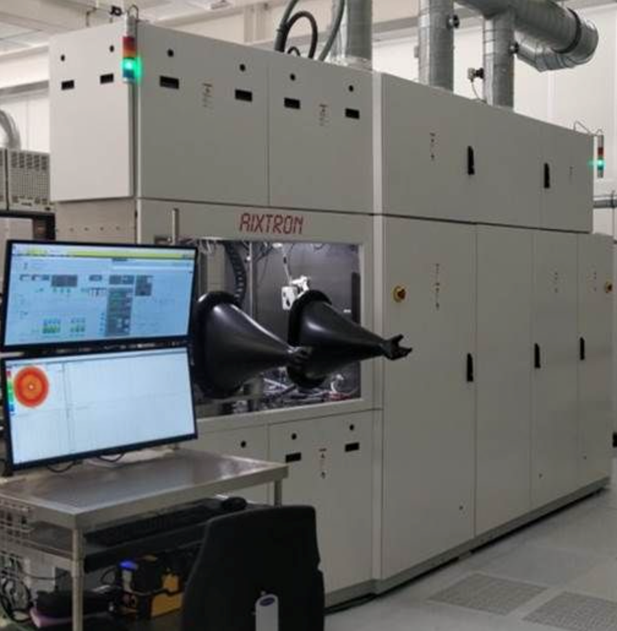
New tools from partners AIXTRON SE and SUSS MicroTec have been installed in the imec cleanroom. Photo credit: AIXTRON.
Asselberghs: The Graphene Flagship aims to connect academia and industry. How does imec contribute to this goal?
At imec we are uniquely positioned to have access to both: laboratories dedicated to fundamental research and fab infrastructure that adds an industrial dimension. This strategic positioning places us at the intersection of industry and academia.
El Kazzi: How do you see the challenges of the lab-to-fab transition and what are your proposed solutions?
The first challenge for a lab-to-fab transition in my opinion, is miscommunication between industry and academia. Academics feel that companies “Don’t tell me what they need”, and manufacturers think that “Academia lives in a different world.” But I believe the perception on both sides can be wrong.
Now the second challenge has a technical side and it's related to the nature of these materials. They are very thin, down to monolayers, so a slight modification or interaction on their surface changes everything. Therefore, accurate handling and reproducible processes are huge tasks.
This is why AIXTRON is working on these challenges by:
1) Helping our customers and the 2D community to enable new markets for these materials by bringing the top researchers in this field together.
2) Providing the most effective and FAB-compatible reactors that synthesise wafer-scale 2D-materials. A very good example is the MOCVD platform which we have recently installed at imec.
Asselberghs: what is needed to fill the gap between lab and fab?
To effectively bridge the gap between lab and fab, it is important to invest in versatile tools that enable faster screening of materials and processes. This, in turn, ensures an efficient down selection at a moderate cost.
Establishing process maturity is a tedious task, but very much needed. Our approach consists in the selection of materials and processes through accurate metrology inspections correlated with electrical and/or optical read-outs. This approach allows us to generate essential datasets needed to seamlessly transfer information between the industry and academia.
El Kazzi: Tell us more about the MOCVD machine?
AIXTRON is indeed the world leader of MOCVD machines. Realizing that this technique is the most promising for 2D wafer scale integration made us develop a specific tool to synthesise these films. The MOCVD process usually involves the deposition of semiconductor materials onto a substrate, typically a wafer, to create various structures. Our machine operates by introducing volatile metal-organic precursors and other gases into a heated reaction chamber, resulting in the deposition of the desired material onto the substrate.
AIXTRON machines specifically offer precise control over deposition parameters, for example the temperature can range from room temperature to 1200oC for 300 mm, allowing for the customisation of material properties and the growth of high-quality epitaxial layers.
Our machine has other unique features such as closed coupled shower head, double injection lines, and thus the possibility to grow single and 2D heterostructure materials. Lastly, I think one of the most important features is our transfer module which will allow the growth of 2D on 300 mm wafers like Si, sapphire, etc.
Asselberghs: What are you mostly excited about?
We are looking forward to using this 200/300 mm compatible MOCVD reactor to continue our work on transition metal dichalcogenides (TMDCs), in particular sulphide-based TMDCs. I am excited to see the first 300mm deposition on 300mm sapphire wafers within the 2D-EPL project.
Additionally, IMEC has recently also installed a SUSS 200/300 mm compatible automated tool for the delamination of TMDCs from the growth substrate. The availability of these unique tooling allows us to take the next step forward in the set-up of matured modules for 2D-material growth and layer transfer: both are essential modules in establishing pilot-line process capability.
El Kazzi, are you taking part in Graphene Week 2023?
Yes, I will present on Thursday 7 September at the 11.30 session “Plenary Session 7: Graphene Flagship 10 years”. Also, AIXTRON sponsored the cake to celebrate the 10 years of the Graphene Flagship. Our colleague Michael Heuken however will also present on the 2D-EPL project on Thursday afternoon.
Asselberghs: will you be there as well?
Definitely, and we will present our recent updates of the 2D-EPL project on Thursday afternoon. I hope to see you all in Gothenburg!
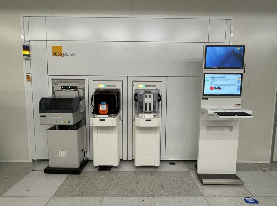
New tools from partners AIXTRON SE and SUSS MicroTec have been installed in the imec cleanroom. Photo credit: AIXTRON.
Author bio

Letizia Diamante
Science Writer and Coordinator of the 'Diversity in Graphene' initiative.