Light bends electrons through graphene
Graphene Flagship researchers from ICFO in Barcelona, in collaboration with teams in Columbia University, US, NTU, Singapore and NIMS, Japan, have reported the first use of light to bend of electrons in bilayer graphene.

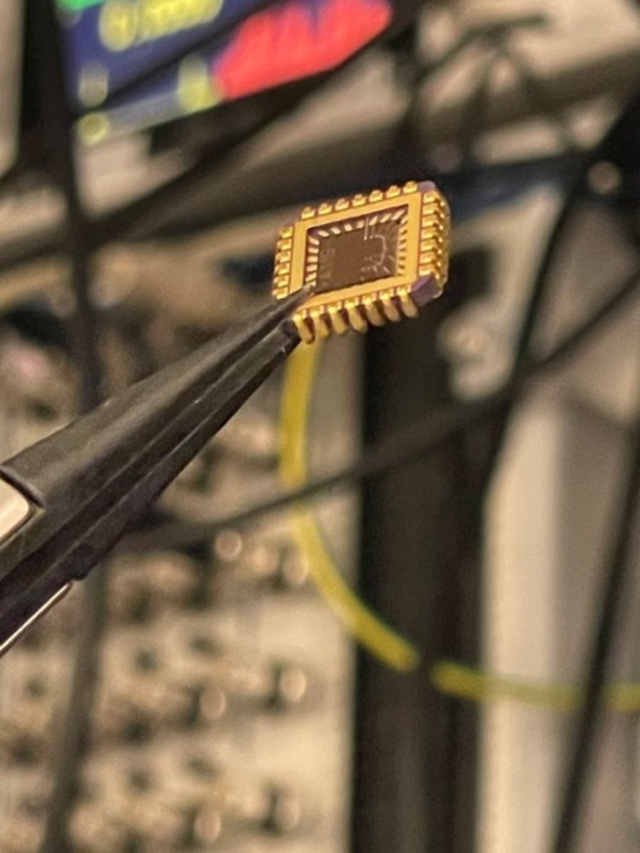
Close-up of one of the devices used for the experiment carried out by Jianbo Yin and colleagues. Image credit: ICFO.
Such discovery could have major implications in applications for imaging in space, medical imaging, and even security applications such as the quality inspection of new materials.
Graphene Flagship Leader for Photonics and Optoelectronics
The way electrons flow in a material determines its electronic properties. For example, when a voltage is applied across a conducting material, electrons start flowing, generating an electrical current. Some electrons flow in straight paths, moving along the electric field, like a ball rolling downhill. Yet, these are not the only trajectories electrons take: when a magnetic field is applied, the electrons bend. Such bent electron flows lead to transverse signals called Hall responses.
Now, is it possible to bend electrons without magnetic fields? In a study recently published in Science, Graphene Flagship researchers, and collaborators in the US, Singapore, and Japan, used circular polarised light to induce bent electronic flows in bilayer graphene.
Jianbo Yin, first author of the study based at Graphene Flagship partner ICFO, remembers how it all started. “This collaborative study began in 2016 with a conversation a scientific conference. Electrons are not just particles, they also have a quantum wave-like nature”. In layered quantum materials, such as bilayer graphene, the wave pattern of electrons can exhibit a complex winding often referred to as quantum geometry. “We talked about the possibility of harnessing quantum geometry in bilayer graphene to bend the flow of electrons with light instead of using magnetic fields”. With this in mind, the team decided to take on the challenge of experimentally realising this unusual phenomenon.
In bilayer graphene, there are two pockets of electron valleys: when a perpendicular electric field is applied, the quantum geometrical properties of electrons in these two valleys cause them to bend in opposite directions. As a result, their Hall effects are cancelled out.
In this study, scientists found that by applying circular polarized infrared light onto the bilayer graphene device, they were able to selectively excite one specific valley population of electrons in the material, which generated a photovoltage perpendicular to the usual electron flow.
Frank Koppens, co-leader of the study and Graphene Flagship Leader for Photonics and Optoelectronics based at Graphene Flagship partner ICFO highlights: ”We engineered the device and setup in such a way that current only flows with light illumination. With this, we were able to avoid the background noise that hampers measurements and achieve a sensitivity in the detection several orders of magnitude better than any other layered materials.” This development is significant because conventional photodetectors often require large voltage biases that can lead to “dark currents” that flow even when there is no light.
Yin remarks that “we can control the bending of the electrons with the out-of-plane electric field we apply. We can change the bending angle of these electrons, which can be quantified by the Hall conductivity. By controlling the voltage ‘knob’, the Berry curvature [one characteristic of quantum geometry], can be tuned, which can lead to a giant Hall conductivity.”
The results of the study open a new realm of many detection and imaging applications, says Koppens. “Such discovery could have major implications in applications for infrared and terahertz sensing since bilayer graphene can be transformed from semimetal to semiconductor with a very small bandgap, so it can detect photons of very small energies. It may be also useful, for example, for imaging in space, medical imaging, e.g. for tissue skin cancer, or even for security applications such as the quality inspection of materials”.
The possibilities are manifold and the next steps of research focused on new layered materials, such as the moiré material twisted bilayer graphene, may find new ways of controlling electron flows and unconventional opto-electronic properties.
Gianluca Fiori, Graphene Flagship Division Leader for Electronics & Photonics Integration, says: “The physical effect demonstrated in the article represents a clear milestone in the field. Indeed, it could have important implications also in the ICT field, opening the path towards the exploitation of the valley degree of freedom of carries in order to transfer and elaborate information. The fact that electrical signals due to valley polarized carries can be modulated through an external electrical electric field could enable novel photodetectors and electronic devices. This work, led by researchers of the Graphene Flagship, highlights also the importance of international collaborations, where complementary expertise have been put together within a synergic action, and which has been the key for success for obtaining this bold result.”
Andrea C. Ferrari, Science and Technology Officer of the Graphene Flagship and Chair of its Management Panel, adds: “This milestone publication as a result of a collaboration between the Graphene Flagship and leading institutions in the US, Singapore and Japan, showcases the breath of the Graphene Flagship reach, seeded with many international workshops over the years. It also confirms how photonics and optoelectronics are key areas for research and application of graphene and related materials. Most importantly, it paves the way for a variety of novel devices targeting tuneable low energy detection, key for many imaging applications.”
Reference
Tunable and giant valley selective Hall effect in gapped bilayer graphene, Jianbo Yin, Cheng Tan, David Barcons-Ruiz, Iacopo Torre, Kenji Watanabe, Takashi Taniguchi, Justin C. W. Song, James Hone, Frank H. L. Koppens. Science, 2022, DOI: 10.1126/science.abl4266.


