Electronic Devices
Sustainable more than Moore devices
The Electronic Devices Work Package strives to obtain sustainable devices with improved capabilities and performance that go beyond the established Moore's Law using graphene and other layered materials.
The last 10 years
Over the last 10 years, the Electronic Devices Work Package has moved its focus from the development of critical process technologies to the realisation of different integrated circuits for logic, radio frequency electronics and flexible electronics. This increase in complexity was only possible by laying the foundations at the beginning of the Graphene Flagship, putting sufficient effort toward fabricating reliable and reproducible devices.
Over time, the focus has moved from graphene to other layered materials, such as semiconducting transition metal dichalcogenides (TMDs), especially molybdenum disulphide (MoS2), which have great potential for electronic applications.
Thanks to the versatility of layered materials, we modelled and demonstrated how to print traditional CMOS devices onto flexible substrates, such as paper, for environmentally friendly electronics. Other advances include high data-rate communication links, new Hall sensors for position sensing and electronic devices for biomedical applications.
In addition, the Work Package experienced a clear transition from focusing on “hero devices” to the optimization of the reproducibility and reliability of fabrication processes, to progress the large-scale production of electronic devices in Europe.
This year’s progress
The know-how acquired this year around the reliability and reproducibility of our transistors put these technologies a step ahead in the realisation of complex circuits based on layered materials. This is a huge result, inconceivable ten years ago.
In particular, the researchers also improved the stability of graphene-based field-effect transistor devices by adjusting the energy level of the charge carriers, so that they are less likely to interact with the defects in the insulator without needing to reduce the total number of defects.
The Electronic Devices Work Package made progress in non-volatile resistive switching made from monolayer molybdenum disulphide in a metal-insulator-metal structure, which could be used to create analogue switches for high-frequency communications. They can operate at 100-500 GHz frequencies, which correspond to the 6G communication band.
Finally, we reported that hexagonal boron nitride (h-BN) can be used as a barrier layer between MoS2 and a commonly used encapsulation layer, aluminium oxide (Al2O3). This barrier layer prevents charge transfer from Al2O3 to MoS2 and helps to protect MoS2 from environmental factors. The resulting devices are more stable and show lower hysteresis.

Daniel Neumaier, Work Package Leader
Our new technologies can open new scenarios in the field of electronics and be the key for the much-needed shift towards next-generation high-performance and low-power devices.”
Work Package Leader
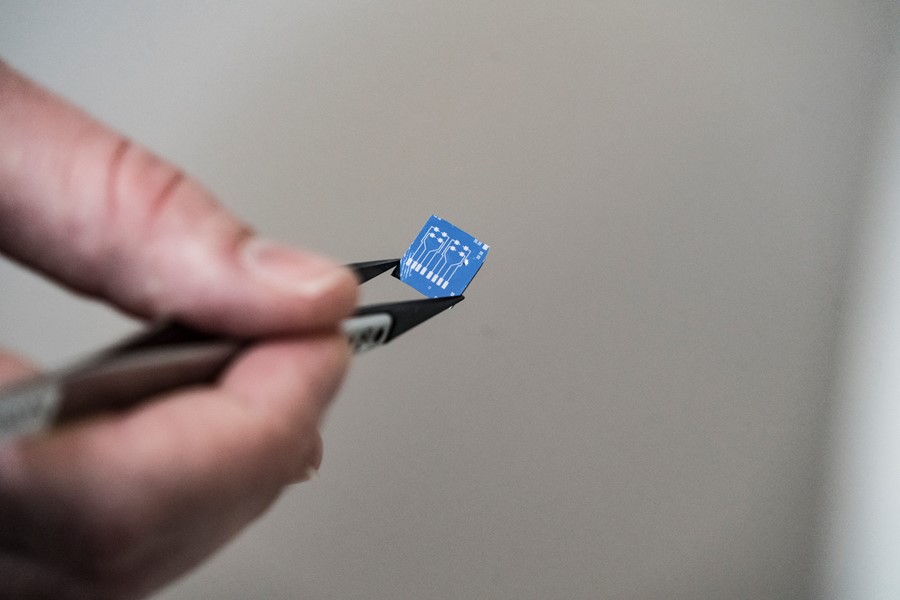
An early chip produced by the Electronic Devices Work Package. Credit: Johan Bodell, Chalmers University of Technology
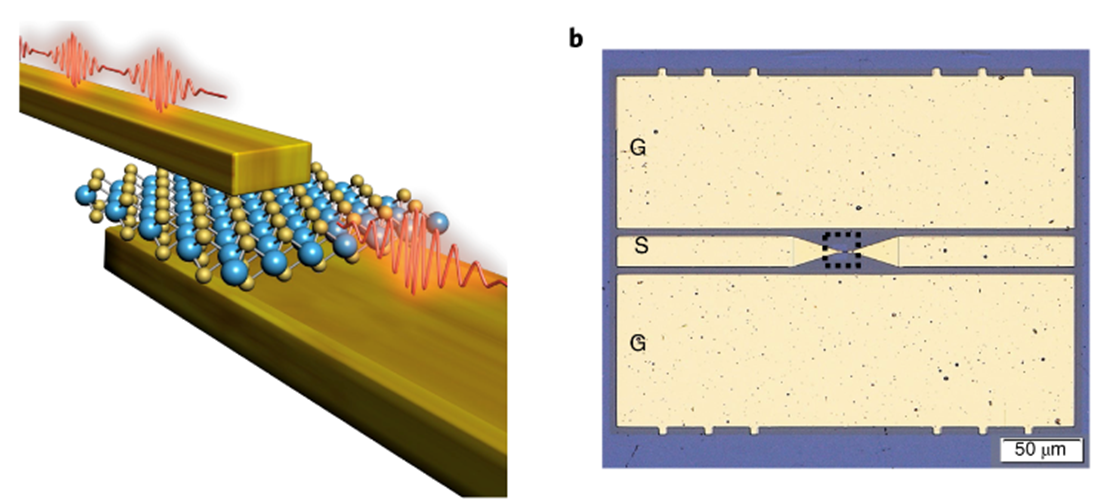
A simplified illustration of a radio frequency switch with a vertical metal–insulator–metal structure and monolayer MoS2 as the resistive switching insulator (left). Optical microscopy image of a fabricated monolayer MoS2 radio frequency switch where the dashed box shows the vertical metal–insulator–metal structure (right). Credit: Nature Electronics
References
Kim, M. et al. Nat. Electron, 2022, DOI: 10.1038/s41928-022-00766-2
Knobloch, T. et al. Nat. Electron, 2022, DOI: 10.1038/s41928-022-00768-0
Piacentini, A. et al. Adv. Electron. Mater. 2022, DOI: 10.1002/aelm.202200123
Latest Articles

Stretching the Limits of Graphene with Robin Smeyers

2D-PL funded to further mature 2D material wafer-scale integration
Launched in October 2024, the Graphene Flagship’s 2D-Pilot Line (2D-PL) project aims to further strengthen the European ecosystem in the development of integration modules for photonics and electronics prototyping services.

The commercialisation of graphene electronics
Kari Hjelt and Henning Döscher of the Graphene Flagship, have collaborated on a new article published in Springer Nature Electronics titled: “The commercialisation of graphene electronics.”

GATEPOST project celebrates its first anniversary
All eight European partners in the GATEPOST project celebrated a particularly pleasing event at the last six-monthly meeting. The project, funded by the European Commission through Horizon Europe, the European Framework Programme for Research and Development, has an ambitious goal. The development and production of a new type of graphene-based chip is intended to turn existing computer technology and IT security upside down and revolutionise them," explained Dr Mindaugas Lukosius of IHP GmbH Leibniz Institute for Innovative Microelectronics and lead partner in the project.

First photonic integrated GATEPOST chip
First major milestone achieved in the EU GATEPOST project: All eight European project partners from industry and science meet to discuss the progress of the project and reflect on the development work of the last six months.

2D-EPL OFFERS A NEW EXPERIMENTAL MPW FROM GRAPHENEA SEMICONDUCTOR
Multi project wafer (MPW) runs are a common practice within the semiconductor ecosystem. Universities, R&D centres and start ups, which usually only need a few prototypes and operate with tight budgets, take advantage of this service to obtain devices at an affordable entry point. This is carried out with a mask sharing scheme, where devices with different geometries but shared device architecture are manufactured within the same mask; in this way, everyone gets a few devices but no one needs to purchase more devices than necessary. Now, Graphenea partners with the 2D Experimental Pilot Line (2D-EPL) to offer an MPW run with a novel process flow.