Photonics and Optoelectronics
Graphene for high-speed communications
The Photonics and Optoelectronic Work Package focuses on research areas and high technology readiness level (TRL) activities that provide fast solutions for data-transmission, image sensing technologies and terahertz (THz) detection at room temperature, which are difficult to achieve with traditional electronic and optical technologies.
The last 10 years
As graphene has evolved from components to application-tailored prototypes over the past decade, the objectives of the Work Package have followed the same trajectory. We launched five spin-offs (i.e., Camgraphic, Emberion, Cambridge Raman Imaging and Qurv) stemming from the research and development efforts of the Work Package. These meet the needs of different industries, and target optical sensors, imaging systems and data communications.
In particular, Cambridge Raman Imaging is developing a coherent Raman microscopy platform, based on the graphene-enabled dual wavelength fibre laser source, that can differentiate between cancer and healthy tissues. Preliminary chemometric data of tumour tissue samples have been acquired and the product is expected to be launched as soon as the end of 2023, targeting the market of cellular process analysis in academia and pharma/biotech industry. Then the product will evolve into a clinical scanner to assess tissue biopsies and support histopathologists in the process of diagnosing cancer.
During Core 3, some of the activities with higher TRL moved to the Graphene Flagship Spearhead Projects linked to data communication and broadband image sensors. In the Work Package, we aim to develop the best performing building blocks, while the work carried out in the Spearheads focuses on engineering innovative solutions. By the end of 2023, we aim to surpass state-of-the-art devices and target end-user specifications with the motivation to advance the TRL of these systems even further in the future.
This year’s progress
Over the past year, the researchers in the Photonics and Optoelectronic Work Package worked on THz lasers and detectors. They produced a THz quantum cascade laser (QCL) working at 55% of its total possible range of frequencies. This ability, known as "comb operation", is useful for detecting harmful gases and explosives and can be applied to infrared imaging systems to detect medical conditions, breath analysers and a variety of other sensing and spectroscopic applications.
The team also reported room temperature detectors for THz frequencies using CVD-grown, large-area, single-layer graphene, integrated in antenna-coupled field effect transistors. The device showed quick responses (around 5 nanoseconds) and low levels of background noise.
Finally, the scientists discovered a way to generate a photovoltage perpendicular to the usual electron flow by shining circularly polarized light on a bilayer graphene device. This new energy source can be used for detecting small amounts of light and energy, which could have important applications in fields like infrared and terahertz sensing, space imaging, medical imaging and material inspection for security purposes.
Frank Koppens, Work Package Leader
We have seen new applications of graphene emerging almost unpredictably.”
Work Package Leader
References
Riccardi, E. et al. Laser Photonics Rev. 2022, DOI: 10.1002/lpor.202200412
Di Gaspare, A. et al. Adv. Opt. Mater. 2022, DOI: 10.1002/adom.202200819
Asgari, M. et al. Appl. Phys. Lett. 2022, DOI: https://aip.scitation.org/doi/full/10.1063/5.0097726
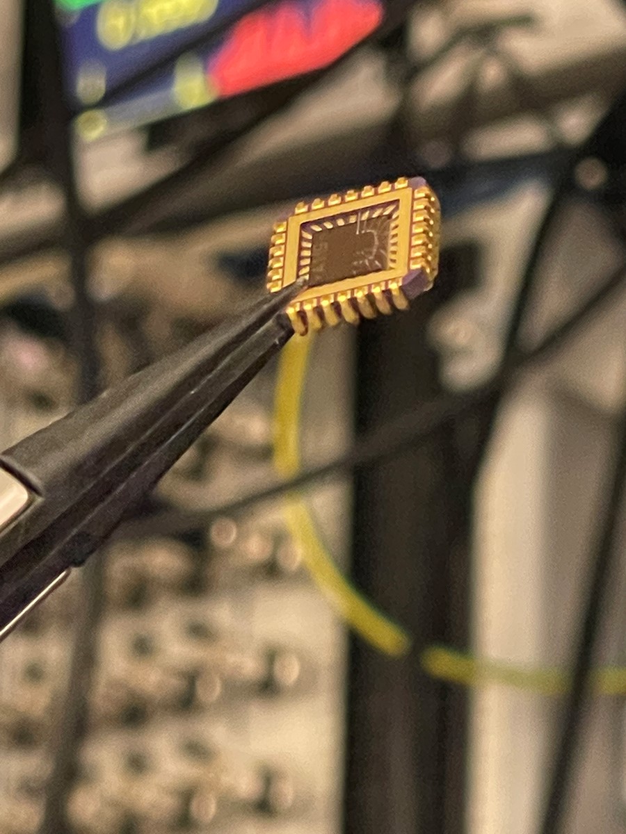
Device prepared by the Photonics and Optoelectronic Work Package. Credit: ICFO
Latest Articles

€211M funding positions CamGraPhIC to break AI’s data barrier

2D Pilot Line Showcases Next-Gen Semiconductor Integration at SEMICON Europa
The 2D Pilot Line (2D-PL) presented its work on integrating two-dimensional materials (2DM) in semiconductor technologies at SEMICON Europa 2025, held at the Munich Messe on 18-21 November 2025. The project — part of the Graphene Flagship — is accelerating the transition of 2DM from lab-scale research toward real industrial integration in photonics and electronics.

2D-PL launches support programme for for MPW runs
Customers of the 2D Pilot Line's (2D-PL) multi-project wafer (MPW) runs can now apply for a 50% reduction in fees in exchange for providing feedback to help the project improve its processes.

2D-PL funded to further mature 2D material wafer-scale integration
Launched in October 2024, the Graphene Flagship’s 2D-Pilot Line (2D-PL) project aims to further strengthen the European ecosystem in the development of integration modules for photonics and electronics prototyping services.

GATEPOST project celebrates its first anniversary
All eight European partners in the GATEPOST project celebrated a particularly pleasing event at the last six-monthly meeting. The project, funded by the European Commission through Horizon Europe, the European Framework Programme for Research and Development, has an ambitious goal. The development and production of a new type of graphene-based chip is intended to turn existing computer technology and IT security upside down and revolutionise them," explained Dr Mindaugas Lukosius of IHP GmbH Leibniz Institute for Innovative Microelectronics and lead partner in the project.

Graphene and 2D materials in photonics: A revolutionary leap in technology
In the vast landscape of modern science and technology, graphene and two-dimensional materials (2DM) have emerged as game-changers, revolutionising industries with their remarkable properties and diverse applications. Among the myriad fields benefiting from their extraordinary characteristics, photonics stands out as one of the most promising domains. Photonics, the science and technology of generating, detecting and controlling photons, has found new avenues for innovation and advancement through the integration of graphene and 2D materials. In this article, we delve into the captivating realm of photonics and explore how graphene and 2D materials are reshaping its landscape, opening up unprecedented possibilities and paving the way for groundbreaking discoveries.