


Synergistic effects of graphene flakes
Graphene Flagship researchers produced graphene fragments with a diameter smaller than 100 nm – and showed their potential for photodetection.
Researchers at the Graphene Flagship Partners University of Strasbourg and LuMIn, Université Paris-Saclay (CNRS, France) and Graphene Flagship Associated Member University of Nova Gorica (Slovenia), produced graphene fragments with a diameter smaller than 100 nm – and showed their potential for photodetection.
Different layered materials are often piled up in a specific way to boost the functionality of the overall system. The Graphene Flagship team decided to combine graphene with graphene flakes and exploit the optoelectronic properties of this device.
The Graphene Flagship researchers adapted the technique used to break the weak interactions between graphite sheets and produce graphene. Extending this approach, they exfoliated graphene aggregates to single-layer, semiconducting graphene flakes. Such small flakes are akin to molecules, and self-assemble on the graphene surface, forming highly ordered structures, known as superlattices, with the molecules oriented parallel to the graphene substrate. This arrangement forms strong interlayer bonds and improves graphene’s properties.
The Graphene Flagship team then tested a photodetector made of single-layer graphene covered with graphene flakes, reaching high responsivity and detectivity, comparable to the highest values obtained with graphene-metal photodetectors. These findings demonstrate the synergy of graphene layers with graphene flakes for high-performance, low-toxicity optoelectronics.
“We keep combining molecular science with layered materials to boost graphene properties and impart new functions to layered materials. Our ultimate goal is to achieve multi-responsive, multi-functional, ‘more-than-Moore’ devices,” says Paolo Samori of the University of Strasbourg, who led this study.
“This is an elegant strategy to fabricate functional graphene-nanographene van der Waals heterostructures that can provide unique functions, in the current case, the fabrication of a state-of-art photodetector device. The strategy in this work can certainly be expanded to other emergent layered crystals which enable the construction of multi-functional devices,” says Xinliang Feng, Graphene Flagship Leader for Functional Foams and Coatings.
Andrea Ferrari, Science and Technology Officer of the Graphene Flagship and Chair of its Management Panel, adds: “This is a very interesting result, exploiting electron confinement in nanometre scale graphene flakes, on top of large area graphene, to obtain state of the art photodetectors. This showcases the versatility of graphene and how its properties can be tailored by changing its shape and size. Yet again the Graphene Flagships opens a new research area with great potential for applications”.
Reference
Liu, Zhaoyang, et al. "Solution-processed graphene–nanographene van der Waals heterostructures for photodetectors with efficient and ultralong charge separation." Journal of the American Chemical Society (2021).
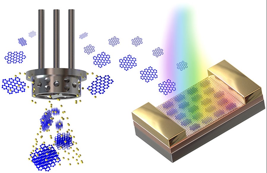
Graphene flakes boost the effects and properties of graphene-based optoelectronics. Credit: JACS / American Chemical Society.
Author bio

Letizia Diamante
Science Writer and Coordinator of the 'Diversity in Graphene' initiative.