Large scale imaging of the electrical quality of graphene
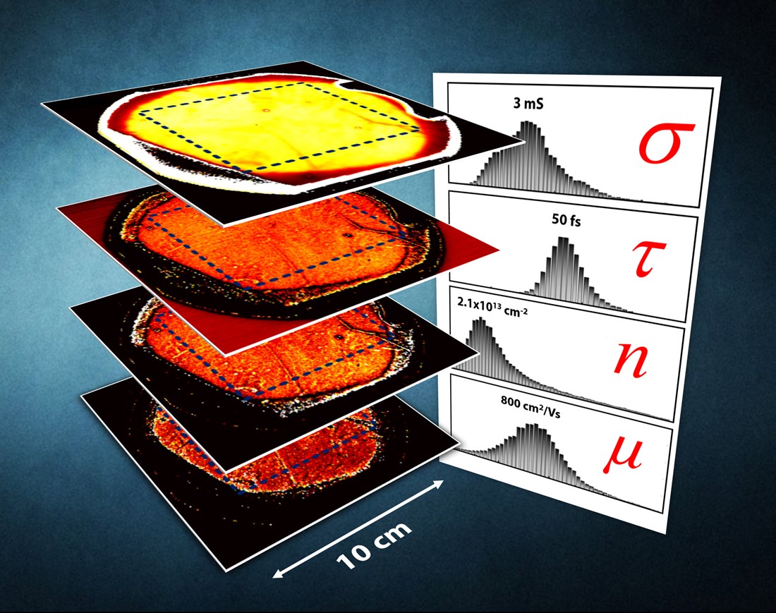
Terahertz time-domain spectroscopy conductivity mapping of graphene.
Researchers from the Graphene Flagship developed a new technique to map the conductivity of graphene on the large scale. This technique uses the non-destructive, fast and highly accurate terahertz time-domain spectroscopy and has exciting ramifications for the graphene production environment.
As the industrialisation of graphene requires its production at even larger scales, techniques to characterise its electronic properties in real time are of utmost importance, to ensure the necessary quality control required by industry. Large area sheets of graphene are nowadays needed for many applications in electronics, communications, photovoltaics and much more. Thus, their characterisation techniques need to be not only quick but reliable and, importantly, non-destructive.
“Large scale metrology is going to be an integral part of industrialisation,” said Professor Peter Bøggild, Group Leader at DTU Nanotech and the paper’s lead author, “We will never get real quality without quality control”.
In this article, Professor Bøggild, Professor Peter Uhd Jepsen (DTU Fotonik) and others assess the current state of the art of graphene conductivity characterisation techniques. Common to many of these is a trade-off between speed, availability, accuracy and scale. While electrical device measurements using lithographic contacts give accurate and reliable information, the process is cumbersome and results in destruction of the graphene film. Four point probes are less destructive, but too slow and impractical in terms of mapping large areas.
In contrast, time-domain spectroscopy (THz-TDS) is ideally suited for large scale characterisation. It is a non-destructive technique where the absorption of terahertz radiation is measured across a graphene film without physical contact, providing fast, accurate information of the electrical “quality” in real time at the large scale.
“Due to the relevance of the method for the electrical characterisation of graphene films the International Electrotechnical Commission (IEC) has incorporated THz-TDS into its work programme. Under the involvement of international technical experts, the IEC will develop a standard for industrial use. This standard is prerequisite for acceptance of the method for quality assurance in the graphene industry,” said Dr Norbert Fabricius from Karlsruhe Institute of Technology, Germany, Secretary of the IEC Technical Committee 113 and Leader of Standardisation within the Graphene Flagship.
From the lab to the production environments THz-TDS can be used to analyse graphene conductivity. Importantly, as graphene finds its way into different industrial environments THz-TDS also enables the mapping of carrier density and carrier mobility along with conductivity at rates that far exceed the commonly used methods, and are relevant even for a high-throughput roll-to-roll scenario. THz-TDS determines the absorption of long-wavelength terahertz radiation by the graphene film, which gives a very precise measurement of the conductivity. With a spot size of 0.1-0.5mm this allows visualisation of the large-scale uniformity as well as the statistics to support development of high quality and highly consistent graphene materials, required by industrial applications.
Bøggild confirms that the method works well with graphene on flexible, transparent polymers and even allows measurement of graphene sealed underneath a protective layer. “With this work we want to advance characterisation, metrology and quality control, and ultimately show that graphene should be taken seriously by industry. Within the Graphene Flagship we collaborate with world-class facilities such as Aixtron in Germany, NPL and Cambridge University in UK and IMEC in Belgium, to verify the technique for a number of different uses. Our next goal is to map the electrical properties of square-meters of graphene. We are also working with DasNANO, who manufacturers THz conductivity mapping equipment, and KIT in Germany, to define a new metrology standard for measuring the conductivity of graphene,” said Bøggild.
Professor Andrea C. Ferrari, Science and Technology Officer of the Graphene Flagship, and Chair of its Management Panel, added “The development of large scale techniques for the industrial characterization of graphene is of paramount importance in the road from lab to fab. The work of Flagship Partner DTU firmly puts Europe at the forefront of this strategic innovation area. Companies worldwide are screaming for standardised and reproducible graphene samples on large area and this novel approach could be deployed on the production floor as validation tool.”


